IBM Unveils World's First 2nm Chip with Nanosheet Tech, Intel and Samsung to Benefit
50 billion transistors in a tiny chip
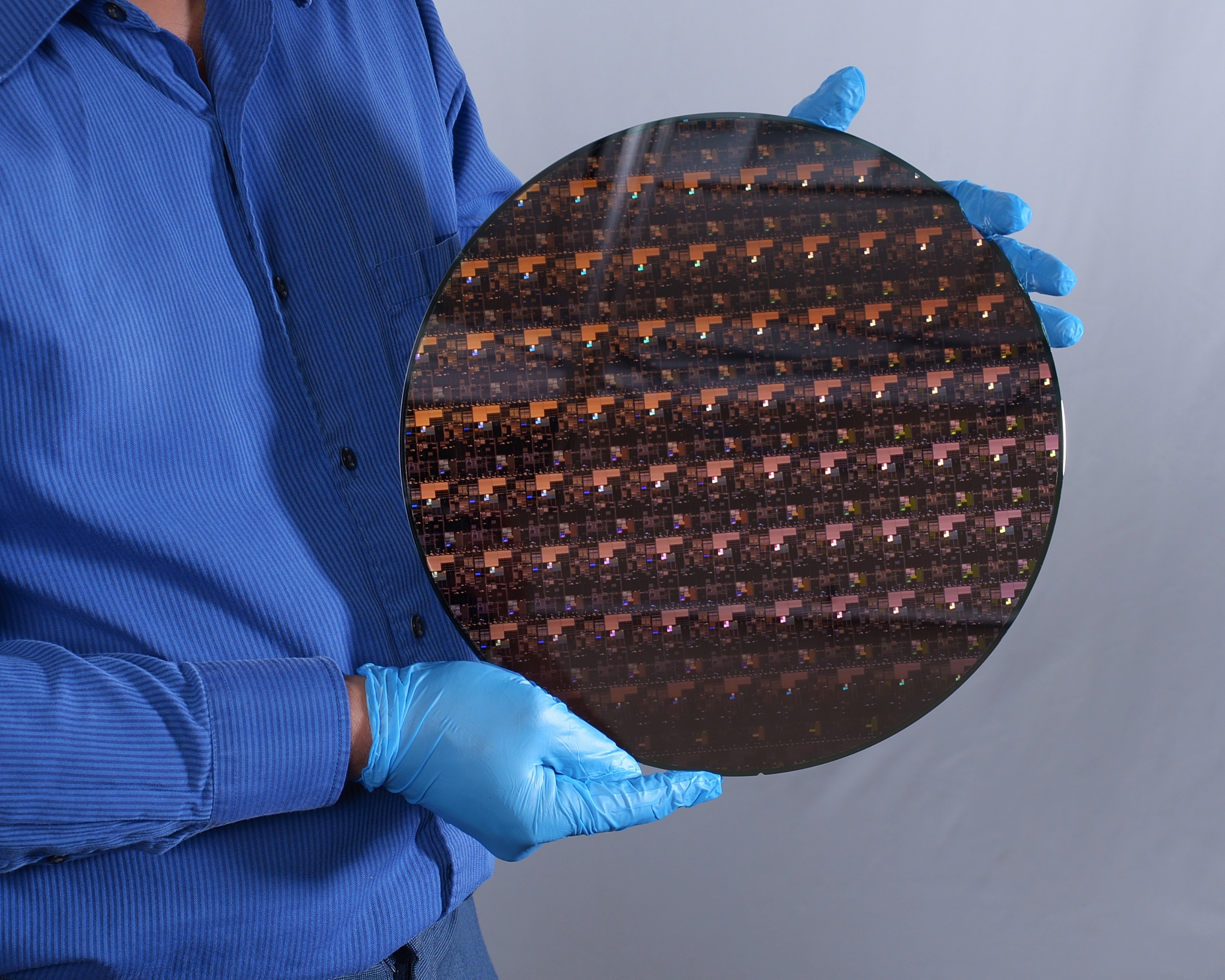
IBM research unveiled a new 2nm chip with nanosheet technology today that will serve as the underpinning of its future process technology. IBM displayed a full 300mm wafer produced on the 2nm nanosheet process at its Albany, New York facilities. However, it is important to remember that the technology is still in the research phase, so the wafer doesn't have productizable chips, at least in their current form.
IBM no longer mass-produces processors; instead, it helps develop technology for its partners, like Intel and Samsung. The former recently announced that it would research new process node and packaging technologies with IBM as part of its new IDM 2.0 initiative. That means that Intel's future 2nm chips could be based on some of these IBM breakthroughs, and there are plenty.
IBM claims that the new process node tech will improve performance by 45% using the same amount of power or 75% less power while maintaining the same performance as today's 7nm processes.

IBM says the new chips will feature up to 50 billion transistors in a chip the 'size of a fingernail' but hasn't provided transistor density metrics (MTr/mm2) that would give us a better sense of how density compares to other modern chips.
However, as with all modern chip node naming conventions, it's important to remember that the '2nm' metric isn't tied to a specific physical feature on the chip. Instead, it's developed based on the power consumption and performance of comparable process nodes from third-party foundries, meaning that modern chip nanometer naming is largely a marketing exercise. That's an industry-wide problem that isn't confined to IBM, though.
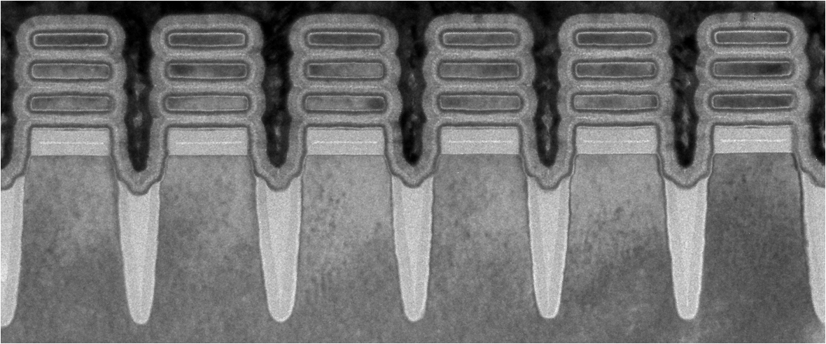
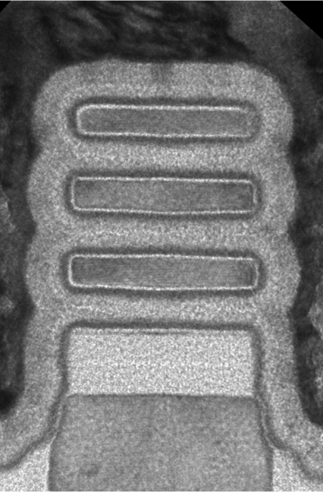
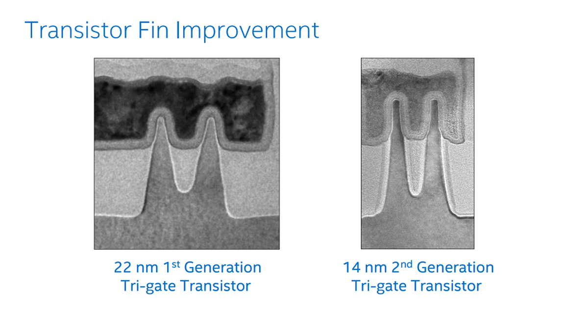
The first image in the album above shows a cross-section of six of IBM's 2nm transistors. If you're accustomed to looking at electron microscope cross-sections of transistors, you'll notice these are markedly different from the third image, which is Intel's current-gen 14nm FinFET technology.
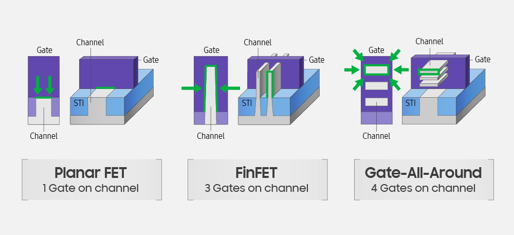
IBM's new design consists of three stacked horizontal silicon nanosheets, with each nanosheet surrounded entirely by a gate. This 'gate-all-around' (GAA) technique reduces voltage leakage that prevents switching off the transistors. This is becoming more of an issue as transistors shrink — even when the gate surrounds the channel on three sides, as we see with FinFET transistors (illustrated in the final image).
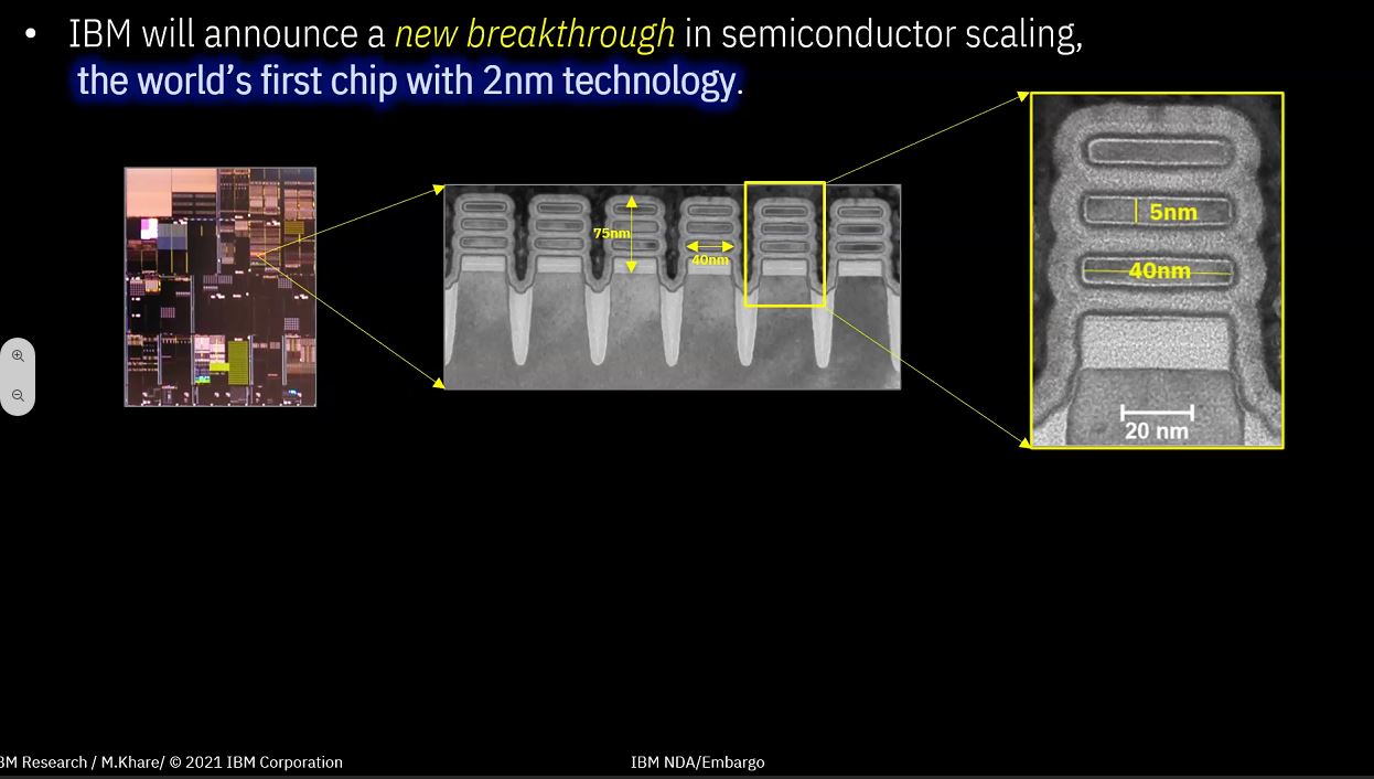
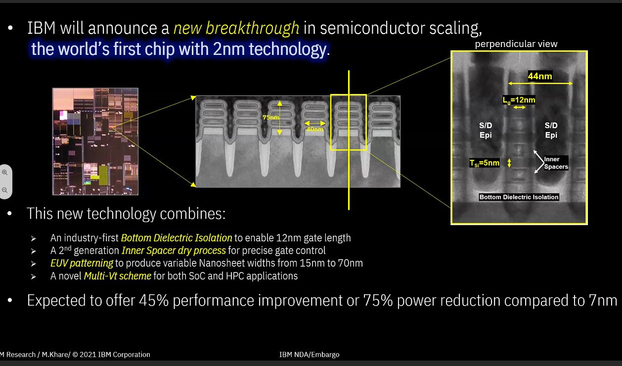
Here we can see IBM's slides on its 2nm nanosheet transistors and the various measurements. Each transistor has three stacked nanosheet layers surrounded by gates, and the entire stack measures 75nm tall in aggregate. Each nanosheet measures 5nm x 40nm with a 12nm gate length, and the transistor has a 44nm pitch.
IBM has made several other notable steps forward with the tech, including the industry-first Bottom Dielectric Isolation to eliminate leakage current from the first nanosheet in the stack, enabling the 12nm gate length. IBM isn't sharing further details on the materials it uses in the 2nm process, such as if it uses silicon-germanium, but the company says it will share more details in the future.
IBM's 2nm process is also the first to use EUV lithography on the front-end-of-line (FEOL) portion of the chip where the transistors and associated structures are created (nanosheets and gate). In contrast, currently-shipping transistor technology uses EUV patterning in the middle-of-line (MOL) and back-end-of-line (BEOL) stages that comprise the interconnects and packaging portions of the chip, respectively.
Surprisingly, IBM says that it uses single-exposure EUV in every critical layer of the chip, including FEOL, reducing complexity (fewer optical masks and steps) and improving yields compared to multi-patterning. This technique can create nanosheet widths from 15nm to 70nm, giving the fabs some flexibility with cell libraries and SRAMs based on various design targets. IBM also disclosed that it uses the Twinscan NXE:3400B EUV machine from ASML to produce its 2nm test wafers.
IBM ran its own chip-producing facilities for roughly 25 years before selling that portion of its business to GlobalFoundries back in 2014. However, IBM has continued its own research and development and licensing of its core technologies through its $3 billion 'Seven Nanometers and Beyond' research program that the company began after it sold its fabrication facilities. Samsung has been the company's key partner, a relationship that will continue in the future with IBM's process technology. In fact, Samsung will produce IBM's own Power10 processors this year on a 7nm process developed in conjunction with IBM.
Intel's announcement that it will collaborate with IBM on future logic and packaging technologies came as an understated overly-broad statement in its IDM 2.0 announcement a little over a month ago. However, the partnership holds momentous importance for Intel as it looks to recover from years of stagnation with its process technologies, and IBM was quite clear in our briefing that its new 2nm tech will benefit all of its partners, which includes Intel.
IBM has only shared the basic details of its 2nm nanosheet design, so there's still much to learn, such as how the company plans to tackle interconnect scaling, which has become a key hurdle in the path to smaller transistors. Simply put, the smallest transistors in the world are of no use if you can't wire them together, and that has been one of the most pressing constraints to shrinking to smaller nodes.
Additionally, IBM hasn't shared details around SRAM, density metrics for the various cell libraries, or the materials it uses for the 2nm node. We expect all these questions, and hopefully more, to be answered as we worm our way to the first products based on the tech. IBM says it expects its 2nm nanosheet process to roll out of partner foundries in late 2024, but it didn't give any firm projections which foundries would lead the way with tech based on its research.
Get Tom's Hardware's best news and in-depth reviews, straight to your inbox.

Paul Alcorn is the Editor-in-Chief for Tom's Hardware US. He also writes news and reviews on CPUs, storage, and enterprise hardware.
-
VforV Reply
I guess you didn't read the article... you would have seen that IBM is partnering with both Samsung and Intel to "give" them this new 2nm tech.peachpuff said:Intel: oh yeah? Well we have 10nm...
If it's indeed true, I'm more worried for AMD because of this... both nvidia (from Samsung) and Intel would benefit. -
Krotow ReplyVforV said:I guess you didn't read the article... you would have seen that IBM is partnering with both Samsung and Intel to "give" them this new 2nm tech.
If it's indeed true, I'm more worried for AMD because of this... both nvidia (from Samsung) and Intel would benefit.
TSMC are researching 2 nm for 2 years already. So AMD will be not left behind here. I would not care about Nvidia - they are miner hardware manufacturers now. -
Sippincider ”Hey Intel and Samsung! We have a big breakthrough in 2nm and these chips are gonna be SWEET!”Reply
”Cool. How are we gonna build them in volume?”
”Oh details details, you always gotta find fault in the details….” -
VforV Reply
I hope AMD won't be behind... as for Nvidia being a miner GPU provider, that is very much true, but they won't abandon gaming and lying to gamers that they care about them, thus fooling enough people to buy their overpriced GPUs - when they can.Krotow said:TSMC are researching 2 nm for 2 years already. So AMD will be not left behind here. I would not care about Nvidia - they are miner hardware manufacturers now. -
Drazen As I'm aware Samsung promised GAA this year at their 5nm node. And this will be first GAA. TSMC plans FinFET for new few years.Reply
Looks 2nm cause TSMC investigates 3nm. -
Porsche Dan ReplyVforV said:I guess you didn't read the article... you would have seen that IBM is partnering with both Samsung and Intel to "give" them this new 2nm tech.
I guess you didn't read the PR that this article was shamelessly mashed from. Samsung already has 2nm in production and TSMC has it in the lab. And it will be a cold day down below before Intel licenses a process technology from anyone much less IBM.
You should also Google the 5nm announcement IBM made a few years back. That technology also never made it into high volume manufacturing.
If you folks had an ounce of semiconductor experience you would know all of this. But hey, anything for a click. -
VforV Reply
Ok Mr. Knowledge, I guess Ian is a clickbait hunting troll or a clueless tech talker too right?Porsche Dan said:I guess you didn't read the PR that this article was shamelessly mashed from. Samsung already has 2nm in production and TSMC has it in the lab. And it will be a cold day down below before Intel licenses a process technology from anyone much less IBM.
You should also Google the 5nm announcement IBM made a few years back. That technology also never made it into high volume manufacturing.
If you folks had an ounce of semiconductor experience you would know all of this. But hey, anything for a click.
It's only PR BS according to you...
DZ0yfEnwipoView: https://www.youtube.com/watch?v=DZ0yfEnwipo -
PCWarrior The fact that IBM is presenting a “2nm” wafer first doesn’t mean that Intel, Samsung and TSMC haven’t already produced such wafers themselves internally through their own Research and Development process. Also it should be noted that this “2nm” node is comparable to what Intel would call 6nm in their scale. And it is waaaay much easier to build simple transistor structures in the lab than actually make a large scale manufacturing node using the same transistor concept and on top of that be able to build complex architectures and multiple cores in a large die.Reply
I am pretty sure in 2011 Intel produced such kind of demo wafer internally for their 10nm and they also showed a Canonlake wafer in 2017. It took them 6 years to demonstrate a cpu wafer and over a decade to successfully make large cpus in large scale with it. I am not suggesting that the same will happen again (especially given that EUV can now be used) but there is at least a lag of 4-5 years before a technology like this can make it from this stage to mass production. I expect this to be a thing in mid to late 2025.
https://www.anandtech.com/show/16656/ibm-creates-first-2nm-chip -
thGe17 Reply
Most likely a misjudgment. AMD has almost nothing to do with manufacturing. The firm is only a customer like anybody else and therefore relies on what foundries like TSMC offer.Krotow said:TSMC are researching 2 nm for 2 years already. So AMD will be not left behind here. I would not care about Nvidia - they are miner hardware manufacturers now.
And Nvidia is no minor manufacturer. According latest statistics, AMDs share of TSMCs revenue in 2020 was about 3,3 billion US$ whereas Nvidias share was about 3,5 bn. US$. For 2021 the statistic estimates 4,7 bn. US$ for AMD mostly due to SoC production, and Nvidia reduced its volume to 3,0 bn. US$ but they have shifted a large portion of their production to Samsung.
Additionally, which also might be a surprise: Intel with its relatively small outsourced parts is at TSMC almost as large as AMD. Their manufacturing volume was about 2,7 bn. US$ in 2020 and will be about 3,7 bn. US$ in 2021, therefore only the few outsourced parts almost match AMDs complete production at TSMC (CPU chiplets, APUs, GPUs and console SoCs; the only thing missing here is the IOD, which is manufactured at GloFo in 12/14nm).
Apple still is the single largest customer at TSMC according to revenue share: 2020 about 11,0 bn. US$, in 2021 estimated 13,0 bn. US$, but the share cannot be directly transformed into manufacturing volume, because Apple always uses the latest and most expensive node and they additionally pay/support TSMC in their process development. Still their wafer-volume is obviously also much higher than that of AMD.