Intel finally divulged more information about its long-overdue 10nm Ice Lake Xeon processors at Hot Chips 2020, outlining an impressive ~18% IPC improvement and giving us a taste of what's to come for both the company's data center and high end desktop (HEDT) platforms. Intel has long used its Xeon die designs for both its HEDT and data center chips, albeit with slight revisions between the two, meaning the Ice Lake design also gives us a glimpse of what Intel has planned for HEDT in the near future.
After years of delays, Intel's 10nm Xeon Ice Lake chips are a badly needed addition as the company seeks to fend off AMD's EPYC Rome CPUs that continue to chew away at Intel's market dominance in the data center. Intel has slashed Xeon pricing to remain competitive with EPYC Rome, and the company has faced even more challenges in the workstation and HEDT segments, with AMD's Threadripper processors delivering more than twice the number of cores than Intel's finest.
All of these factors make Intel's new Xeon lineup, and the underlying architecture, all the more important as it heads into even more increased competition with AMD's forthcoming EPYC Milan processors, which also debut at the end of the year. With Intel's 10nm SuperFin Sapphire Rapids Xeons not making their way to market until late 2021, the company now turns to its 10nm+ transistors paired with the sweeping architectural changes found in the Ice Lake Xeons.
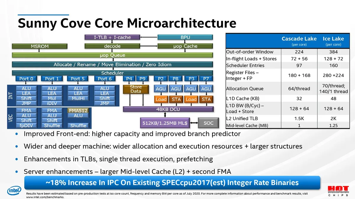


As Intel noted before, the Ice Lake chips will drop into dual-socket Whitley server platforms, while the previously-announced Cooper Lake slots in for quad- and octo-socket servers. Intel's presentation dove into some of the finer-grained architectural optimizations that together yield an ~18% IPC improvement (geomean of SPECIntRate) at the same core count, frequencies, and bandwidth as the Cascade Lake processors (this speaks to the IPC improvement for the Sunny Cove cores, not the SoC). Intel says that Ice Lake's increased frequency and memory bandwidth can uncover even larger IPC gains.
Intel also highlighted a big realignment of the company's 28-core die that also brings along cache, memory, and throughput advances. Notably, Intel didn't divulge the top core counts available with the Ice Lake processors, so we aren't sure if these are the HCC (High Core Count) or XCC (Xtreme Core Count) designs.
Intel fabs Ice Lake on its 10nm+ process, which confusingly isn't the same as its new 10nm SuperFin tech, and etches in Sunny Cove cores that bring a host of new improvements, including wider allocation (5-wide as opposed to 4-wide) and execution units paired with an improved branch predictor. Intel beefed up L2 cache to 1.25MB and improved the transaction lookaside buffer (TLB - 1.5K to 2K entries) while increasing the L1D cache to 48KB and adding a second FMA (consumer Ice Lake chips only have one FMA).
Intel also expanded the out-of-order window (ROB) from 224 to 384 entries [EDIT: Intel clarified this is a typo in the table - the ROB is 352, just like with Ice Lake mobile] and increased in-flight load+store entries to 128+72, as opposed to the 72+56 found on Cascade Lake chips. Scheduler entries were also increased from 97 to 160.
Intel also added support for a host of new instructions to boost cryptography performance, like VPMADD52, GFNI, SHA-NI, Vector AES, and Vector Carry-Less multiply instructions, and a few new instructions to boost compression/decompression performance. All rely heavily upon AVX acceleration, which Intel has also improved dramatically (more below). Intel claims these instructions yield per-core performance improvements ranging from 1.5X to 8X (again, iso clock and core counts) over Cascade Lake (see third slide above).


Intel also made significant alterations to the SoC architecture, which includes a revamped memory hierarchy and I/O subsystem. The coherent mesh interconnect returns with a similar arrangement of horizontal and vertical rings present on the Cascade Lake-SP lineup, but with a realignment of the various elements, like cores, UPI connections, and the eight DDR4 memory channels that are now split into four dual-channel controllers. Intel shuffled around the cores and now has two execution cores on the bottom of the die clustered with I/O controllers (some I/O is now also at the bottom of the die).
Intel claims the shared cache is available to all cores with uniform latency due to the similar alignment of the caching home agent and snoop filter elements. Still, this design also incorporates the two-cycle latency penalty for core traversal between some vertical rows, as opposed to the one-cycle traversal to horizontally-aligned cores.
Intel redesigned the chip to support two new sideband fabrics, one controlling power management and the other used for general-purpose management traffic. These provide telemetry data and control to the various IP blocks, like execution cores, memory controllers, PCIe/UPI controllers, and the like. This is akin to AMD's Infinity Fabric, which also features a sideband telemetry/control mechanism for SoC structures.
The die includes a separate peer-to-peer (P2P) fabric to improve bandwidth between cores, and the I/O subsystem was also virtualized, which Intel says offers up to three times the fabric bandwidth compared to Cascade Lake. Intel also split one of the UPI blocks into two, creating a total of three UPI links, all with fine-grained power control of the UPI links. Now, courtesy of dedicated PLLs, all three UPIs can modulate clock frequencies independently based on load.
PCIe 4.0 also makes its late appearance to Intel's Xeon lineup, which is a critical need in the face of AMD's EPYC. The four dual-channel memory controllers also now match EPYC channel-for-channel, and now support Intel's Total Memory Encryption (TME) that offers DRAM encryption through AES-XTS 128-bit hardware-generated keys. That also helps address an area where Intel was lacking compared to AMD's EPYC processors, but like AMD's implementation, results in the loss of a 'few' percentage points of performance.
Intel's previous-gen memory controllers supported Optane memory, but it ran at lower speeds than the standard DRAM, meaning the system memory would clock down to match the Optane data transfer rates. Those speeds are now equalized with the 200-series Optane DIMMs.
In tandem with several other optimizations (slide 5), Intel claims Ice Lake offers significant performance improvements in per-core memory bandwidth (slide 6).


Densely-packed AVX instructions augment performance in properly-tuned workloads at the expense of higher power consumption and thermal load. So, Intel's Cascade Lake CPUs drop to lower frequencies (~600 to 900 MHz) during AVX-, AVX2-, and AVX-512-optimized workloads, which has hindered broader adoption of AVX code. As such, Intel's changes to its AVX implementation are surely welcome.
Intel has recharacterized its AVX power limits to minimize the frequency impact, thus yielding (unspecified) higher frequencies for AVX-512 and AVX-256 operations. This is done in an adaptive manner based on three different power levels for varying instruction types, as outlined in the first slide. This nearly eliminates the frequency delta between AVX and SSE for 256-heavy and 512-light operations, while 512-heavy operations have also seen significant uplift. This is a tremendous improvement that should foment broader adoption for Intel's latest instructions.
Intel also reduced its P-state transitions, which is the latency involved with core power-state transitions, through 'fairly instantaneous' operation. Intel recorded a reduction from 12us to ~0us, which is a tremendous improvement. Intel made a similarly-impressive reduction to mesh frequency transitions by almost 3X, and reduced typical C6 exit latencies by 30%.
In aggregate, Intel's Ice Lake-SP looks to be a big step forward, and while the performance enhancements look great on paper, the truth is always in the silicon that actually comes to market. We also know that AMD will bring its own massive enhancements paired with (at least) an industry-leading 64 cores to market with its AMD EPYC Milan processors. Both lineups debut at the end of the year. As such, pricing and availability will be key as Intel rolls out its Ice Lake-SP lineup.
