Hot Chips 2017: Intel Deep Dives Into EMIB
Interconnects may be a dry subject to some, but they're the fundamental underpinnings of today's processor architectures. Interconnects are becoming even more relevant as the industry grapples with the waning Moore's Law, and Intel has yet another new interconnect in the works that purportedly offers improvements over existing packaging technology.
It's already been a busy year on the interconnect scene; Intel unveiled its new mesh architecture, and AMD also pushed its Infinity Fabric-powered designs out to market. Those designs will power the company's respective products for years to come.
At the annual Hot Chips semiconductor conference, Intel presented the company's new EMIB (Embedded Multi-Die Interconnect Bridge), which is a complicated name for a technique that provides high-speed communication between several chips. The packaging technology allows Intel to assemble Lego-like components ("chiplets") into single heterogeneous packages.
Article continues belowIntel envisions eventually using EMIB to bring FPGAs, ASICs, CPUs, and HBM memory all onto the same package, possibly ushering in a wave of new customized solutions that wield tremendous compute capabilities.
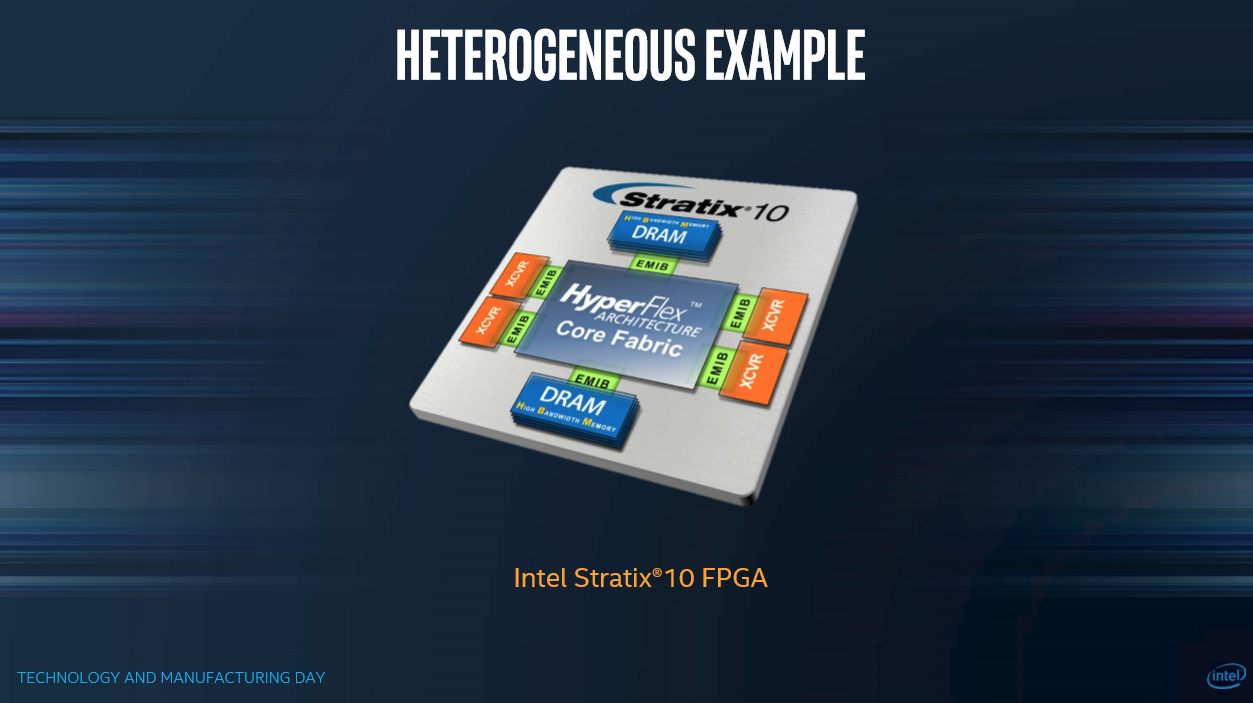
Intel originally painted the new technology in broad strokes during its Manufacturing Day earlier this year, but it dove into more details at the conference. Intel purchased Altera for $16.7 billion in 2015 and folded the FPGA company into its Programmable Solutions Group. Now, Intel is using EMIB packaging for its new Stratix 10 FPGAs, which we'll cover shortly. First, the basics.
Monolithic Versus Heterogenous
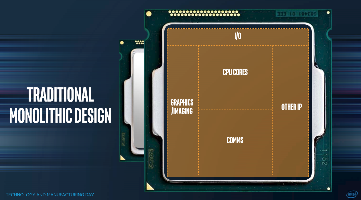
The traditional monolithic die consists of several distinct components, such as CPU cores, I/O controllers, and graphics cores, all manufactured on a single large monolithic die. As chips get physically larger (die area increases), the chance of manufacturing defects increases, thus reducing yields. Also, some components don't scale well to smaller nodes. So, while the 10nm CPU cores may be fully functional, shrinking the I/O controller could be more challenging. Other components are also optimized on certain nodes for specific tasks.
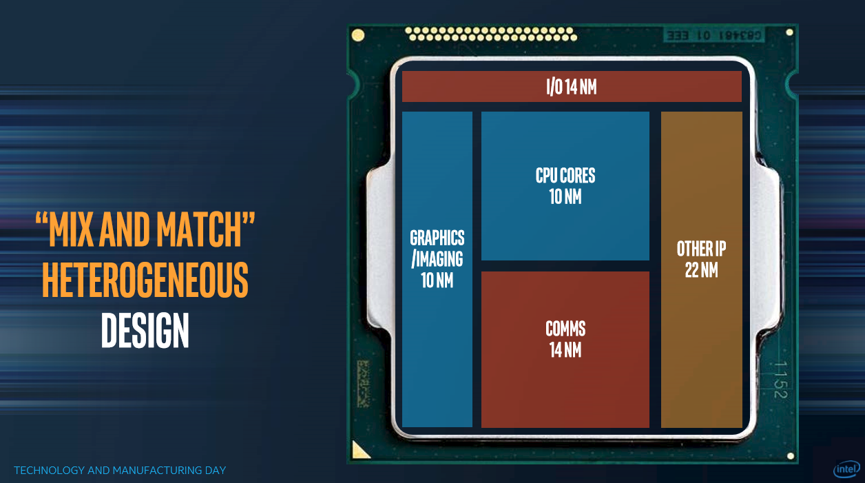
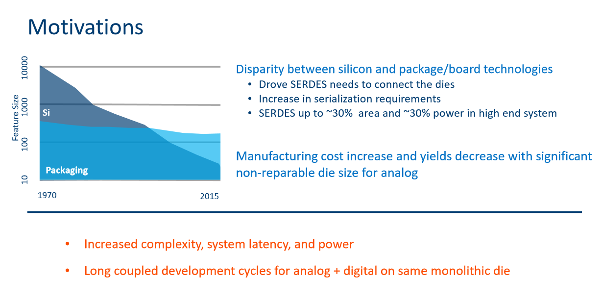
Transitioning to a heterogeneous design, which combines several separate components onto a single package, solves several problems. First, the smaller dies sidestep yield problems by reducing the chance of catastrophic defects. It also allows Intel to combine several different components with different processes onto the same package. That lets the company use larger nodes for the harder-to-shrink or purpose-built components. It also decouples development cycles for analog and digital devices, thus decreasing time to market.
Get Tom's Hardware's best news and in-depth reviews, straight to your inbox.
The idea is simple in concept, but providing a low latency, low power, and high bandwidth interconnect between the components is a major challenge. Doing it at a reasonable cost is even harder.
Building the Heterogeneous Chip
We already see heterogeneous designs with existing processors such as Intel's Knights Landing. Similar techniques are also used for connecting HBM packages to GPUs, such as Nvidia's Volta and AMD's Vega. AMD's EPYC and Threadripper processors also combine several chips into a single logical processor, but the approach is somewhat different because each chip is a fully functioning unit. There are different paths, with varying levels of efficiency and performance, to constructing heterogeneous chips, but Intel claims they aren't as sophisticated as EMIB.
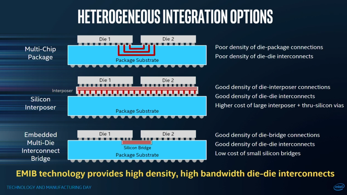
There are two popular high-performance options. The first is a multi-chip package, which connects the die through the package substrate. The design suffers from poor connection density in the substrate and where the interconnects meet the die (notice the spacing of the red lines).
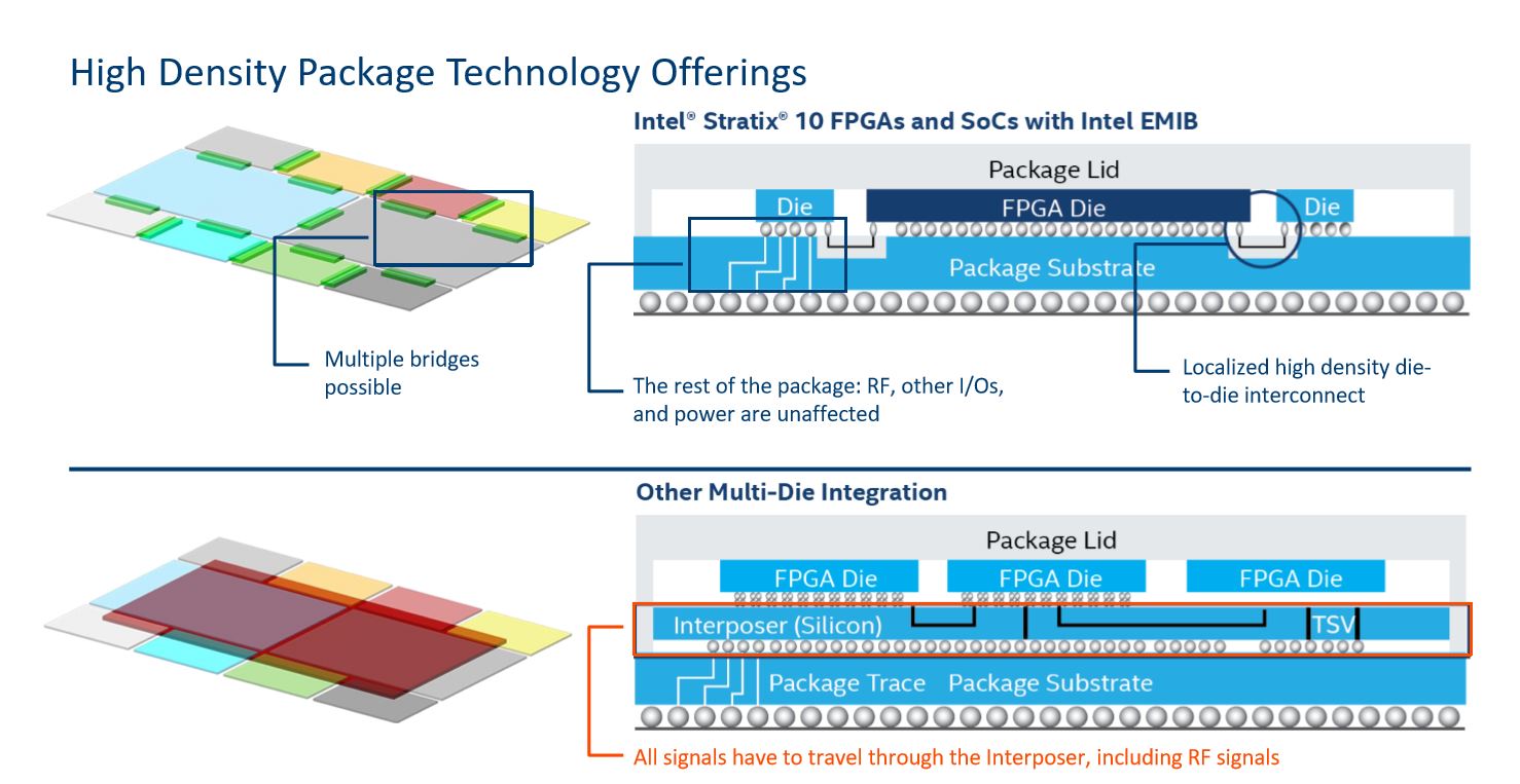
Silicon interposers (2.5D packaging) are another technique. They consist of a thin layer of silicon that slots in between the die and the package substrate. Die-to-die communication occurs through the silicon interposer, which increases connection density. It also improves the die-to-interposer connection density, as well. Unfortunately, silicon interposers are more expensive due to the size of the interposer and TSV technology. Also, all connections on the die have to travel through the silicon interposer, which is important to remember for later. As an aside, AMD's Threadripper and EPYC processors use an organic interposer to connect its Zeppelin die.
Intel's claims EMIB, at the bottom of the slide, solves several issues in one fell swoop. Intel embeds small silicon bridges into the package substrate that allow for tighter interconnect density on the periphery of the die. They also reduce cost because they don't use TSV and are smaller than silicon interposers.
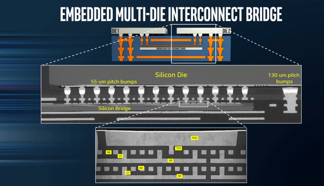
Zooming in on the key areas also unveils another advantage. The silicon bridge features four layers of metal interconnects for die-to-die communication (bottom zoom image). These interconnects have a much tighter pitch than you can achieve with a package substrate.
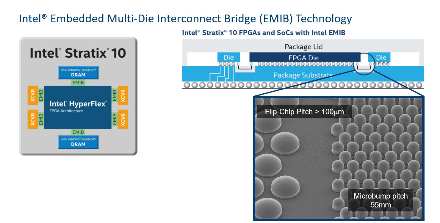
The microbumps on the periphery of the die connect to the silicon bridge and feature a 55-micrometer pitch, which Intel claims will scale down to 35 with next-gen products. 10-micron microbumps are also on the seven-year roadmap. So, there is room to grow. Or shrink, rather.
The remainder of the connections feature a standard >100-micrometer Flip-Chip pitch.
Silicon interposers are large, so all of the traffic, including RF signals, I/O, and power have to travel through them. EMIB transmits digital signals only across the smaller microbumps into the silicon bridge, while other signals still travel through the package substrate. That allows for increased silicon bridge density, and it reduces noise. As pictured above, each package can have multiple silicon bridges. Silicon interposers have size constraints, whereas EMIB-based packages can be much larger.
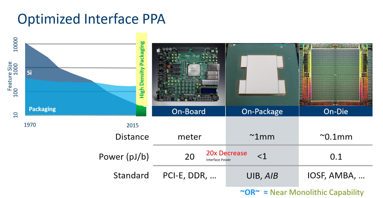
Using EMIB, Intel can package die within 100 microns of one another. That reduces space between the components, which also reduces the power required for data movement. Of course, it still isn't as efficient as an on-die monolithic implementation. At the show, Intel didn't provide power comparisons to standard silicon interposers. Instead, it compared EMIB to standard interconnects, like PCIe and DDR, found on motherboards.
We do know that a single chip can support up to 20,000 EMIB connections with up to 2Gbps of throughput each.
Enter The Chiplet
So, how does this high-speed interconnect impact the Stratix 10 FPGA?
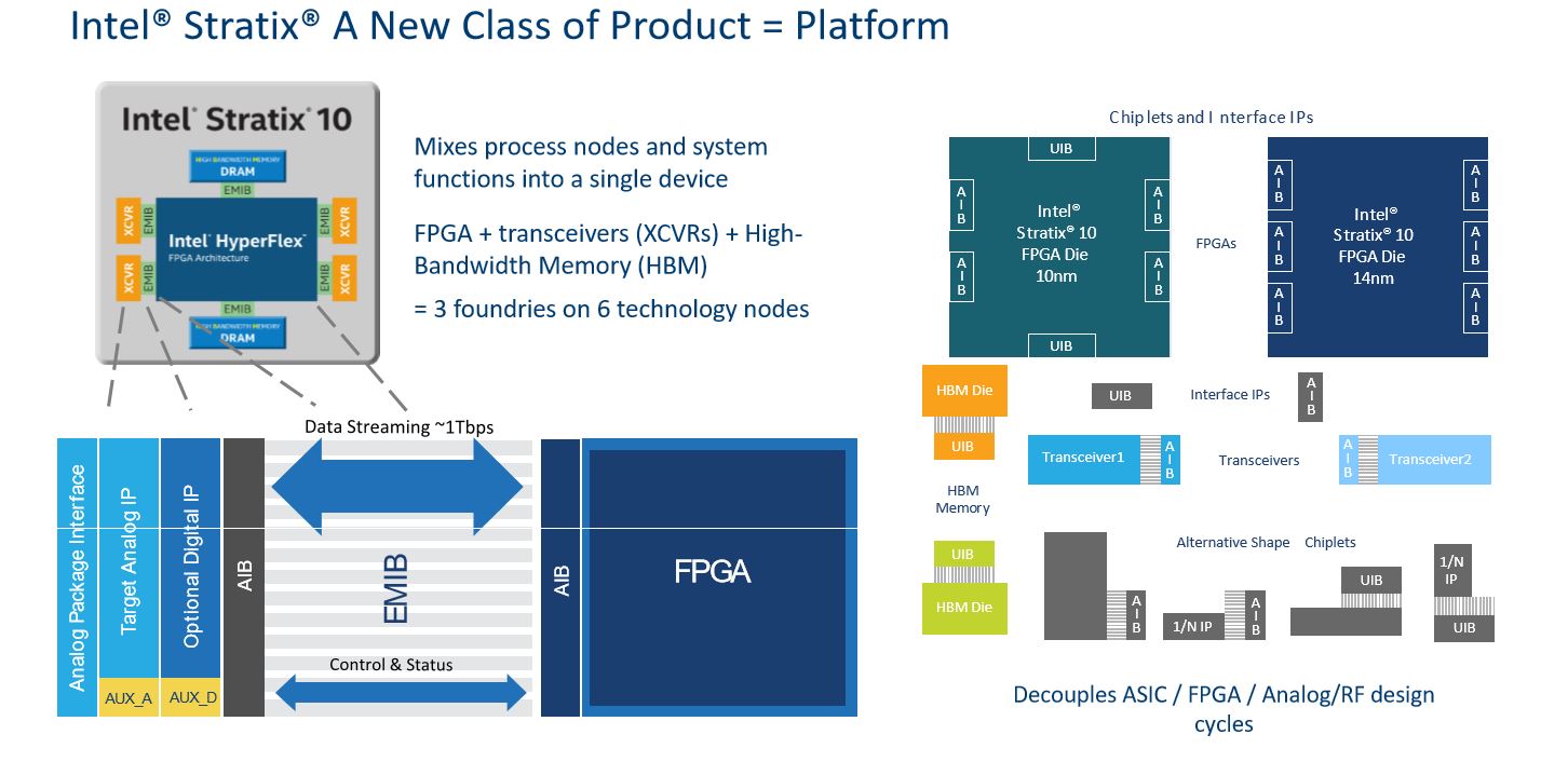
Intel is working with partners to develop chiplets, which are small re-usable IP building blocks that can be processors, transceivers, memory, or other types of components. Intel can mix and match the chiplets, much like Lego blocks, and connect them to the FPGA to create custom designs for different application use-cases.
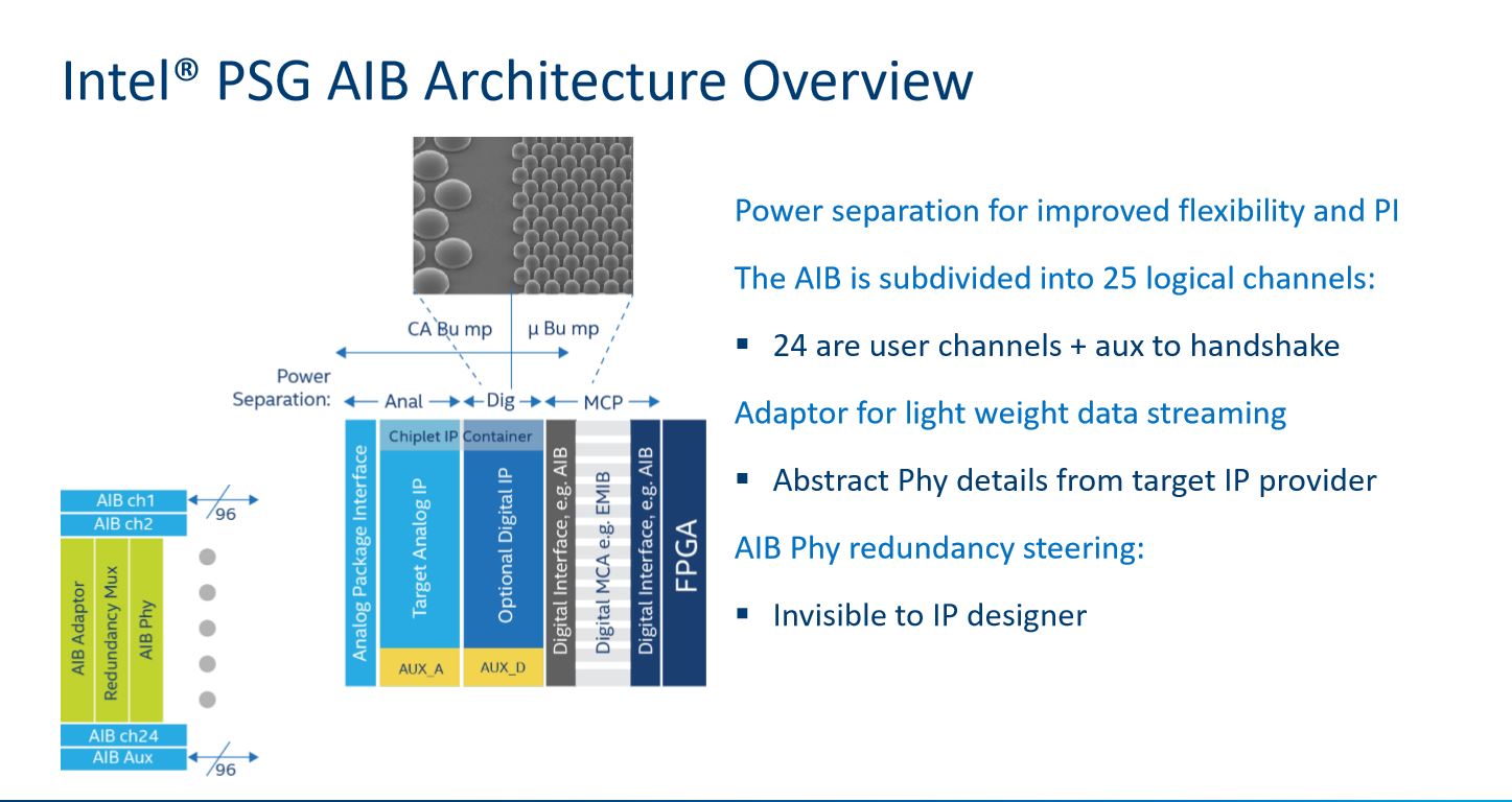
Chiplets are a great idea, but a standardized SiP interface between components is important, especially if other companies are involved in the effort. The AIB and UIB interface IP blocks we see on the Stratix 10 die are the key. UIB connections are a general-purpose SiP interface for HBM and ASICs, while AIB supports transceiver connections and other general-purpose components.
Intel subdivides the AIB PHY into 25 logical channels, with 24 exposed to the user and one dedicated to handshaking operations. We can also see the standard EMIB interface, with the smaller microbumps dedicated to the digital interface while the larger connections handle analog.
Chiplet designers don't have to worry about specialized programming to leverage the interface--Intel claimed it abstracts away the complexity so the designer can focus on IP design. Intel didn't share details on the ostensibly more complex UIB interface, but we do know that both interfaces support up to 2Gbps per physical line (programmable).
These likely won't be open standards, so it is unlikely that we will see other fabs producing similar heterogeneous packages. However, Intel invites others to develop chiplets for its devices. Chiplet verification is also of the utmost importance to ensure reliability, so Intel has developed a framework of governing rules.
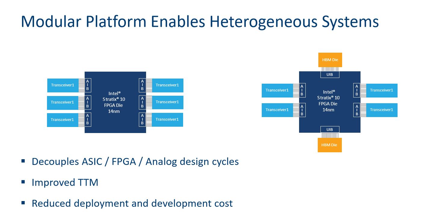
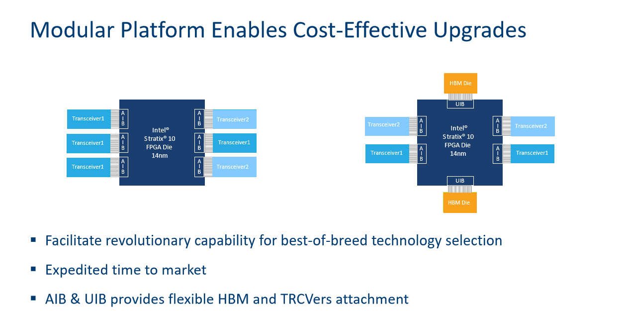
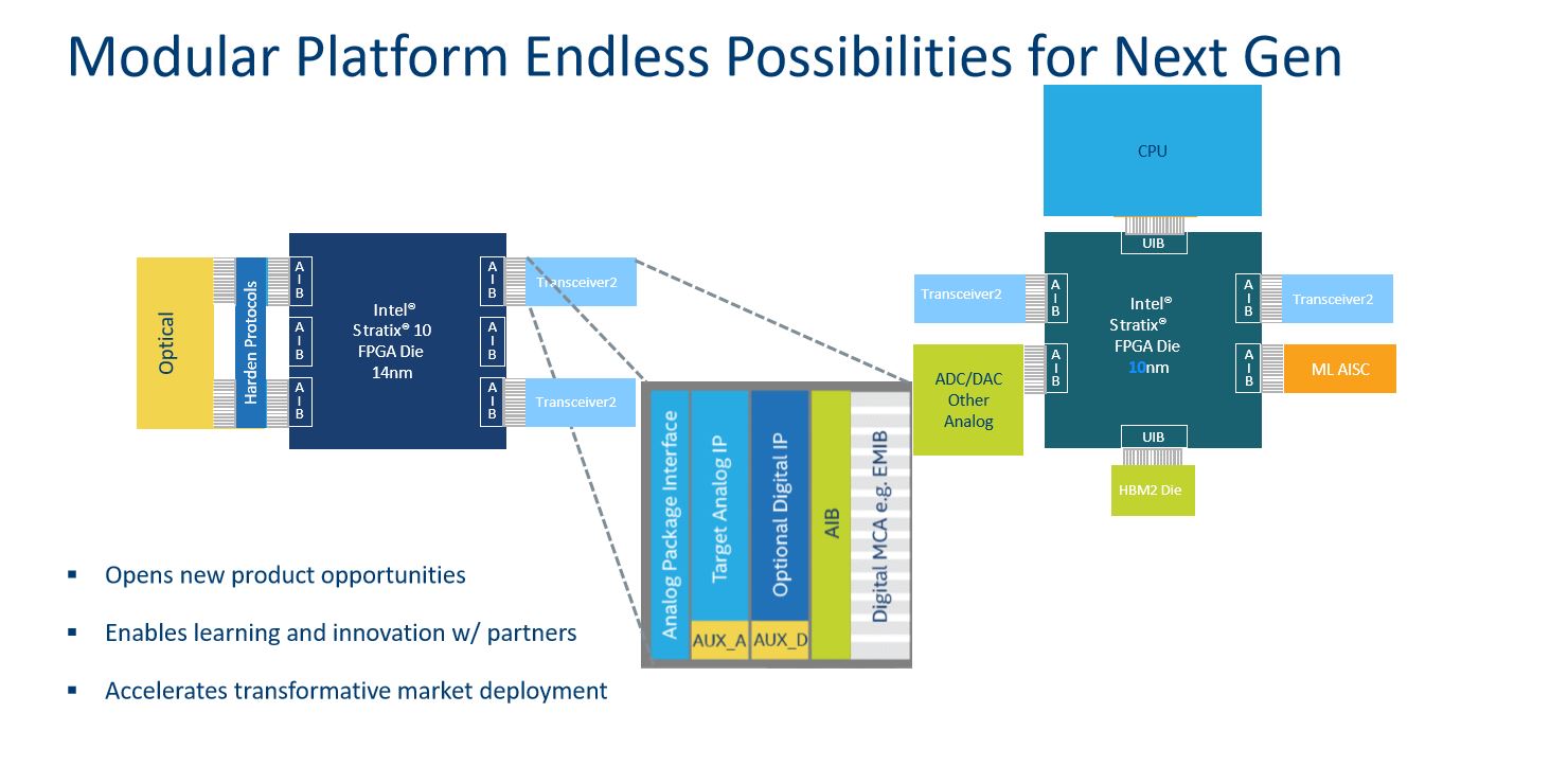
Here we see an example of several different configurations with the Stratix 10 FPGA. One design employs six transceivers, while the other uses four transceivers and two HBM die. The configuration can be armed with many different types of chiplets.
The goal is to eventually create incredible new combinations. As shown on the third slide, you could connect CPUs, HBM, and a machine learning ASIC (think Nervana) to a FPGA to create a homogeneous design. That would be an unheard-of combination with massive performance potential. In fact, the company demoed an experimental FPGA and Skylake combination on the same package last year, so the next generation EMIB interconnect is likely well underway.
Final Thoughts
Intel noted that three different foundries are producing six different technology nodes, and because no single company has a monopoly on innovation, each can create certain customized solutions that are better than their competitors. Building a single monolithic die requires a company to be the best at everything, whereas picking and choosing between chiplets from other vendors allows companies to focus on their core competencies.
Intel plans to expand its EMIB interconnect to its other products--many speculate that EMIB will make its way into the next generation Xeons. Intel hasn't confirmed a specific timeline, but it's only a matter of time. Intel's 3D XPoint will likely come on-package soon, and EMIB appears to be a great fit.
Intel's EMIB has great promise, but it will be costly. Opening the interconnect up as a standard would facilitate faster adoption.
Of course, most of us want to know if it will come to desktop processors as well, but that doesn't seem as likely in the near future. It's logical to assume it might come as Intel pushes the boundaries of Moore's Law.
But Intel, long the keeper of the Moore's Law flame, certainly doesn't want us to think that its new approach is an admission that Moore's Law is waning. The company cited a quote from one of Moore's famed papers (PDF) that states that this type of approach might be an economical solution. Talk about foresight.

Paul Alcorn is the Editor-in-Chief for Tom's Hardware US. He also writes news and reviews on CPUs, storage, and enterprise hardware.
-
redgarl AMD is gluing chips together, however Intel is providing innovation... cmon, they are in pure damage control and they understand they were wrong since Rysen came into play.Reply -
kinggremlin What AMD is doing with their CPU's is not what Intel is developing here. Glue jokes aside, the underlying concept of connecting multiple identical fully functional cpu's to act like a single die higher core cpu like AMD is doing is not new. Intel did that way back with their initial dual core Pentium D and I'm sure they weren't the first.Reply
What Intel is developing with EMIB is more akin to a modular processor. The separate glued together parts (Intel is calling them chiplets) are not the same and do not have to be fully functional processors on their own. Whether or not you want to call it innovative really isn't relevant, because it is a very interesting concept that could lead to the development of products not possible today. -
JamesSneed Reply20103684 said:What AMD is doing with their CPU's is not what Intel is developing here. Glue jokes aside, the underlying concept of connecting multiple identical fully functional cpu's to act like a single die higher core cpu like AMD is doing is not new. Intel did that way back with their initial dual core Pentium D and I'm sure they weren't the first.
What Intel is developing with EMIB is more akin to a modular processor. The separate glued together parts (Intel is calling them chiplets) are not the same and do not have to be fully functional processors on their own. Whether or not you want to call it innovative really isn't relevant, because it is a very interesting concept that could lead to the development of products not possible today.
Honestly its an evolved version on the same concept. AMD will be glueing a Vega core to their Zen cores for their SoC. I get it Intel is making this like it's the best thing ever, showing how they can have different parts with different lithography etc but the AMD way also would allow the Vega to be on 7nm and the Zen core could be on 14nm. Intel is just taking it a step further and allow smaller functional pieces to be "glued" which is pretty interesting but It is a bit ironic that they are taking "gluing" to the next level right after making that a negative point for AMD's Zen based products.
It's rather obvious both sides think monolithic cores are a thing of the past when they start going to smaller process nodes.
-
alextheblue Reply
Well, except for Intel's marketing department.20103761 said:It's rather obvious both sides think monolithic cores are a thing of the past when they start going to smaller process nodes. -
Wisecracker Harmonizing the Industry around Heterogeneous ComputingReply
Let's take a look at the scoreboard:
Advanced Micro Devices & Partners . . . . . . ►77Chipzilla . . . . . . . . . . . . . . . . . . . . . . . . . ►01
( Is there a 75-Run Rule in the IT Industry ? ) -
msroadkill612 Fine, but Intel are just playing air guitar as a spoiler.Reply
We have already seen the sudden appearance of similar "me too" white papers from nvidia re gpu mcmS.
What is the object here? Its to boost HB interlink performance where pcie3 struggles - ie. linking storage/memory/gpu/cpu/nvme.
Clearly, linking the gpu is the greatest mainstream challenge for pcie. Intel do not make a decent GPU, so they are back to square 1 - they have to get nvidia to play ball with a chiplet for intels mcm.
With the imminent release of raven ridge apu, amd will have IN PRODUCTION, examples of these resources interlinked separately& independently from the pcie bus, using the Fabric bus.
Maybe not all in one place, but working examples of having the problem areas covered well & economically, either now or soon.
There is not a lot of other call for chiplets. PCIE handles the low bandwidth details stuff pretty well as is. The real (HB) problems, will have been sorted for millions of happy amd customers long before intels mcm is a reality, in the usual 5 years a fresh product takes.
For example, the pro vega ssg gpu card has 2TB of raid 0 nvme ~storage/cache extender & 16GB of gpu ram. They are all linked on on the discrete vega fabric bus.
Similarly, on amdS imminent apu, we see vega gpu and zen cpu interlinked using infinity fabric.
The age old problem of teaming multi processors, reduces largely to one of maintaining coherency between them.
There is little doubt fabric works excellently at teaming cpuS, judging from Ryzen, & fabric has surely always been planned as including both amds cpu & their gpuS.
AMD have all the ingredients and skills, & are not many steps away from the killer hedt+ product - an APU MCM with multi core cpu, multi gpu, hbm2 cache with nvme ~storage/cache.
If it requires the space of 2x MCMs for high end products, a 2 socket mobo could accommodate that. -
Aspiring techie Now if Intel combines a CPU and 8GB of HBM2 into one package, they could see massive gains in performance using the HBM2 as a last level cache.Reply -
dealcorn Now if Intel combines a CPU and several carefully selected chiplets into one package, they could see massive gains in performance in bunches of application areas.Reply -
Wisecracker Reply... What is the object here? ...
The objective is to productively link disparate processing platforms and peripherals into a power proficient unified 'virtual' computing system.
In other words, everything including the kitchen, sync'd (sorry for the craptastic pun) together under a system arch and OS. Heterogeneous literally means "made up of different parts" that are not uniform.
AMD (and partners) have been slogging away on heterogeneous 'Fusion and 3D-IC' for 10 years now -- including the past 5+ years under the banner of the HSA Foundation. Intel's objective appears to be muddying the heterogeneous waters with proprietary IP -- not the open standards promoted by the HSA partners.
The primary keys to 'bolting together' everything from ARM SoCs, x86 CPUs, programmable chips and SIMD "GPU" compute engines tend to build upon interconnection, coherency, unified memory addressing and OS operability.
