Early Verdict
After many months of building anticipation, AMD is ready to show off Radeon RX Vega 64, and it's...alright. Great 1440p performance and respectable 4K frame rates largely mirror Nvidia's GeForce GTX 1080 at a similar price point. AMD is leaning hard on its FreeSync price advantage and support for features requiring developer support in future games.
Pros
- +
Vega is here, finally
- +
Performance generally similar to GeForce GTX 1080
- +
Future-looking feature set could yield additional performance
- +
FreeSync cost advantage
Cons
- -
High power consumption
- -
Cooling not handled as well as Vega Frontier Edition
- -
Top-billed features await future developer support
Why you can trust Tom's Hardware
Introduction
AMD’s last high-end graphics card launch happened almost 26 months ago. Back then, the Radeon R9 Fury X went toe-to-toe with GeForce GTX 980 Ti and Titan X—the best Nvidia had to offer. And it kept getting better. Subsequent drivers optimized performance, while DirectX 12 helped game developers get more out of the Graphics Core Next Architecture.
Today’s official introduction of the Radeon RX Vega represents the company’s return to high-end gaming, so says AMD. But by its own admission, this isn’t going to be AMD battling for Nvidia’s performance crown. Rather, Radeon RX Vega 64 sets its sights on the performance and pricing of GeForce GTX 1080.
We already know most of what there is to know about Radeon RX Vega 64. AMD made sure of that with a carefully timed sequence of disclosures intended to keep enthusiasts buzzing about its next-gen graphics hardware. In case you missed any of that, check out AMD Teases Vega Architecture: More Than 200+ New Features, Ready First Half Of 2017 and AMD Radeon RX Vega 64: Bundles, Specs, And Aug. 14 Availability.
Today is when we see if the cliffhanger approach to marketing ends with gamers enjoying blissful satisfaction or the pangs of disappointment.
Specifications
Radeon RX Vega 64: At a Glance (Again)
Speeds and feeds are always good to recap, so borrowing from our earlier coverage:
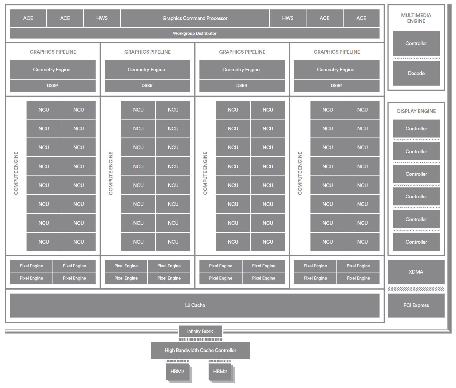
Like the Radeon R9 Fury X's Fiji processor, Radeon RX Vega 64 employs four shader engines, each with its own geometry processor and rasterizer.
Also similar to Fiji, there are 16 Compute Units per Shader Engine, each CU sporting 64 Stream processors and four texture units. Multiply all of that out and you get 4096 Stream processors and 256 texture units.
Get Tom's Hardware's best news and in-depth reviews, straight to your inbox.
Clock rates are way up, though. Whereas Fiji topped out at 1050 MHz, a GlobalFoundries 14nm FinFET LPP process and targeted optimizations for higher frequencies allows the Vega 10 GPU on Radeon RX Vega 64 to operate at a base clock rate of 1247 MHz with a rated boost rate of 1546 MHz. Obviously, AMD's peak FP32 specification of 12.66 TFLOPS is based on that best-case frequency. We typically use the guaranteed base in our calculations, though. Even then, 10.2 TFLOPS is still an almost 20% increase over Radeon R9 Fury X.
The liquid-cooled model steps those numbers up to a 1406 MHz base with boost clock rates as high as 1677 MHz. That’s an almost 13% higher base and ~8%-higher boost frequency, pushing AMD’s specified peak FP32 rate to 13.7 TFLOPS. You’ll pay more than just a $200 premium for the closed-loop liquid cooler, though. Board power rises from 295W on Radeon RX Vega 64 to the Liquid Cooled Edition’s 345W—a disproportionate 17% increase. Both figures exceed Nvidia’s 250W rating on GeForce GTX 1080 Ti, which isn’t even in Vega’s crosshairs.
| Model | Cooling Type | BIOS Mode | Power Profile | |
|---|---|---|---|---|
| RX Vega 64 | Power Saver | Balanced | Turbo | |
| Air | Primary | 165W | 220W | 253W |
| Secondary | 150W | 200W | 230W | |
| Liquid | Primary | 198W | 264W | 303W |
| Secondary | 165W | 220W | 253W |
Speaking of power, our air-cooled sample comes with two BIOS files, and each of those BIOSes supports three power profiles. The primary BIOS at its Balanced power setting is accompanied by a 220W GPU power limit. Dropping to Power Saver cuts GPU power to 165W, while increasing it to Turbo raises the ceiling to 253W. Switching over to the secondary BIOS drops Power Saver to 150W, Balanced to 200W, and Turbo to 230W. We certainly appreciate the granular control AMD enables here, but recognize that most enthusiasts aren't looking for a way to de-tune their $500 graphics card. Regardless, we're planning a follow-up story to explore the effects of each setting on board power, performance, and acoustics.
Each of Vega 10's Shader Engines sports four render back-ends capable of 16 pixels per clock cycle, yielding 64 ROPs. These render back-ends become clients of the L2, as we already know. That L2 is now 4MB in size, whereas Fiji included 2MB of L2 capacity (already a doubling of Hawaii’s 1MB L2). Ideally, this means the GPU goes out to HBM2 less often, reducing Vega 10’s reliance on external bandwidth. Since Vega 10’s clock rates can get up to ~60% higher than Fiji’s, while memory bandwidth actually drops by 28 GB/s, a larger cache should help prevent bottlenecks.
Incidentally, AMD's graphics architect and corporate fellow Mike Mantor says all of the SRAM on Vega 10 adds up to more than 45MB. Wow. No wonder this is a 12.5-billion-transistor chip measuring 486 square millimeters. That's more transistors than Nvidia's GP102 in an even larger die.
Adoption of HBM2 allows AMD to halve the number of memory stacks on its interposer compared to Fiji, cutting an aggregate 4096-bit bus to 2048 bits. And yet, rather than the 4GB ceiling that dogged Radeon R9 Fury X, RX Vega 64 comfortably offers 8GB using 4-hi stacks (AMD's Frontier Edition card boasts 16GB). An odd 1.89 Gb/s data rate facilitates a 484 GB/s bandwidth figure, matching what GeForce GTX 1080 Ti achieves using 11 Gb/s GDDR5X.
As an aside, AMD plans to make its Radeon RX Vega 56 derivative available on August 28th. That 210W card utilizes the same GPU and 8GB of HBM2, but has eight of its Compute Units disabled, eliminating 512 Stream processors and 32 texture units. It'll also run at lower core and memory clock rates. Yet, AMD claims it should outperform GeForce GTX 1070 handily at a $400 price point. Our U.S. lab is in the process of testing Radeon RX Vega 56, and we coverage should follow in the days to come.
Look, Feel & Connectors
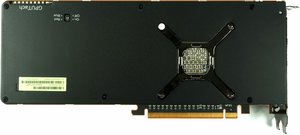
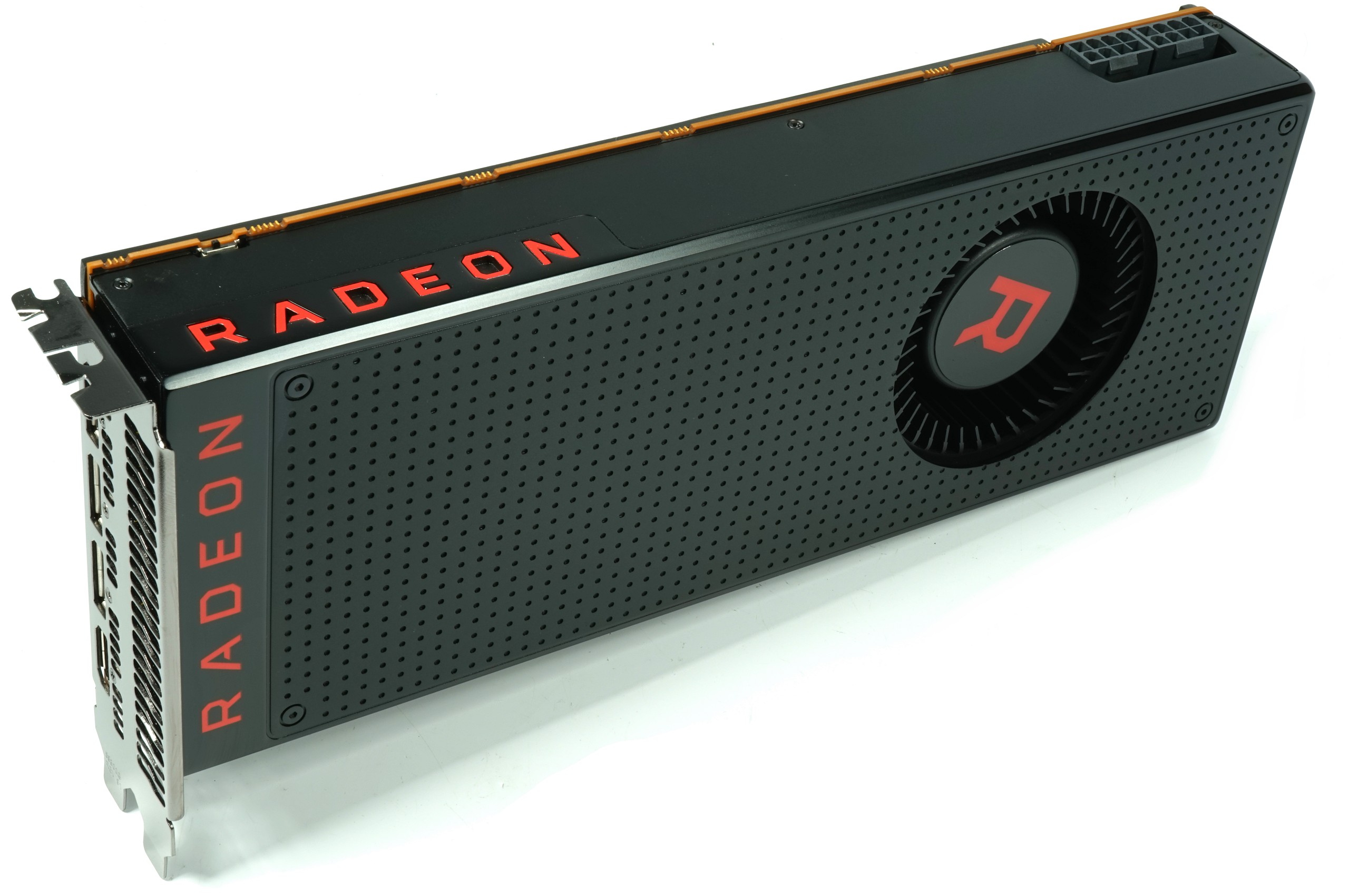
AMD’s RX Vega 64 weighs in at 1066g, which makes it 16g heavier than the Frontier Edition. Its length is 26.8cm (from bracket to end of cover), its height is 10.5cm (from top of motherboard slot to top of cover), and its depth is 3.8cm. This makes it a true dual-slot graphics card, even though the backplate does add another 0.4cm to the back.
Both the cover and the backplate are made of black anodized aluminum, giving the card a cool and high-quality feel. The surface texture is achieved using simple cold forming that preceded the aluminum’s anodization. All of the screws are painted matte black. The red Radeon logo on the front is printed, and provides the only splash of color.
The top of the card is dominated by two eight-pin PCIe power connectors and the red Radeon logo, which lights up. There’s also a two-position switch that allows access to the aforementioned secondary BIOS optimized for lower power consumption and its corresponding driver-based power profiles. These make the card quieter, cooler, and, of course, a bit slower.
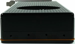
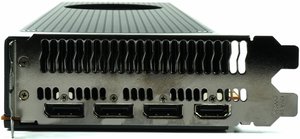
The end of the card is closed and includes mounting holes that are a common sight on workstation graphics cards. The powder-coated matte black slot bracket is home to three DisplayPort connectors and one HDMI 2.0 output. There is no DVI interface, which was a smart choice since it allows for much better airflow. The slot bracket doubles as the exhaust vent, after all.
MORE: Best Graphics Cards
MORE: Desktop GPU Performance Hierarchy Table
MORE: All Graphics Content
-
10tacle We waited a year for this? Disappointing. Reminds me of the Fury X release which was supposed to be the 980Ti killer at the same price point ($649USD if memory serves me correctly). Then you factor in the overclocking ability of the GTX 1080 (Guru3D only averaged a 5% performance improvement overclocking their Vega RX 64 sample to 1700MHz base/boost clock and a 1060MHz memory clock). This almost seems like an afterthought. Hopefully driver updates will improve performance over time. Thankfully AMD can hold their head high with Ryzen.Reply -
Sakkura For today's market I guess the Vega 64 is acceptable, sort of, since the performance and price compare decently with the GTX 1080. It's just a shame about the extreme power consumption and the fact that AMD still has no answer to the 1080 Ti.Reply
But I would be much more interested in a Vega 56 review. That card looks like a way better option, especially with the lower power consumption. -
envy14tpe Disappointing? what. I'm impressed. Sits near a 1080. Keep that in mind when thinking that FreeSync sells for around $200 less than Gsync. So pair that with this GPU and you have awesome 1440p gaming.Reply -
SaltyVincent This was an excellent review. The Conclusion section really nailed down everything this card has to offer, and where it sits in the market.Reply -
10tacle Reply20060001 said:Disappointing? what. I'm impressed. Sits near a 1080.
The GTX 1080 has been out for 15 months now, that's why. If AMD had this GPU at $50 less then it would be an uncontested better value (something AMD has a historic record on both in GPUs and CPUs). At the same price point however to a comparable year and three month old GPU, there's nothing to brag about - especially when looking at power use comparisons. But I will agree that if you include the cost of a G-Sync monitor vs. a FreeSync monitor, at face value the RX 64 is the better value than the GTX 1080. -
redgarl It`s not a bad GPU, however I would not buy one. I am having an EVGA 1080 FTW that I am living to hate (2 RMAs in 10 months), however even if I wanted to switch to Vega, might not be a good idea. It will not change anything.Reply
However two Vega 56 in CF might be extremely interesting. i did that with two 290x 2 years ago and it might be still the best combo out there. -
blppt IIRC, both AMD and Nvidia are moving away from CF/SLI support, so you'd have to count on game devs supporting DX12 mgpu (not holding my breath on that one for the near future).Reply -
cknobman I game at 4k now (just bought 1080ti last week) and it appears for the time being the 1080ti is the way to go.Reply
I do see promise in the potential of this new AMD architecture moving forward.
As DX12 becomes the norm and more devs take advantage of async then we will see more performance improvements with the new AMD architecture.
If AMD can get power consumption under control then I may move back in a year or two.
Its a shame too because I just built a Ryzen 7 rig and felt a little sad combining it with an Nvidia gfx card. -
AgentLozen I'm glad that AMD has a video card for enthusiasts who run 144hz monitors @ 1440p. The RX 580 and Fury X weren't well suited for that. I'm also happy to see that Vega64 can go toe to toe with the GTX 1080. Vega64 and a Freesync monitor are a great value proposition.Reply
That's where the positives end. I'm upset with the lack of progress since Fury X like everyone else. There was a point where Fury X was evenly matched with nVidia's best cards during the Maxwell generation. Nvidia then released their Pascal generation and a whole year went by before a proper response from AMD came around. If Vega64 launched in 2016, this would be totally different story.
Fury X championed High Bandwidth Memory. It showed that equipping a video card with HBM could raise performance, cut power consumption, and cut physical card size. How did HBM2 manifest? Higher memory density? Is that all?
Vega64's performance improvement isn't fantastic, it gulps down gratuitous amounts of power, and it's huge compared to Fury X. It benefits from a new generation of High Bandwidth memory (HBM2) and a 14nm die shrink. How much more performance does it receive? 23% in 1440p. Those are Intel numbers!
Today's article is a celebration of how good Fury X really was. It still holds up well today with only 4GB of video memory. It even beat the GTX 1070 is several benchmarks. Why didn't AMD take the Fury X, shrink it to 14nm, apply architecture improvements from Polaris 10, and release it in 2016? That thing would be way better than Vega64.
edit: Reworded some things slightly. Added a silly quip. 23% comes from averaging the differences between Fury X and Vega64. -
zippyzion Well, that was interesting. Despite its flaws I think a Vega/Ryzen build is in my future. I haven't been inclined to give NVidia any of my money for a few years now, since a malfunction with an FX 5900 destroyed my gaming rig... long story. I've been buying ATI/AMD cards since then and haven't felt let down by any of them.Reply
Let us not forget how AMD approaches graphics cards and drivers. This is base performance and baring any driver hiccups it will only get better. On top of that this testing covers the air cooled version. We should see better performance on the water cooled version that would land it between the 1080 and the Ti.
Also, I'd really like to see what low end and midrange Vega GPUs can do. I'm interested to see what the differences are with the 56, as well as the upcoming Raven Ridge APU. If they can deliver RX 560 (or even just 550) performance on an APU, AMD will have a big time winner there.
