AMD Teases Vega Architecture: More Than 200+ New Features, Ready First Half Of 2017
AMD gathered press and partners late last year to talk about a hectic 2017 roadmap that includes Ryzen for the desktop in Q1; FreeSync 2, new server and laptop platforms launching later in the year; a big push into machine learning; and of course Vega, the hotly-anticipated successor to its third-generation Graphics Core Next (GCN) design.
Let’s cut right to it: Products based on AMD’s high-end Vega GPU architecture aren’t ready yet, but they’re expected sometime between now and the end of June.
In the meantime, AMD is milking this one for all it’s worth. We have early details that the company is willing to disclose, plus a promise that there will be a lower-level tech day closer to Vega’s launch. So let’s dig in (as far as we’re able to go).
Article continues belowRaja Koduri, senior vice president and chief architect of the Radeon Technologies Group, stood onstage at AMD’s Tech Summit and excitedly held up a newborn Vega-based GPU, making a point of the 200+ changes that went into creating Vega. This may be a revision to GCN, but AMD clearly wants the world to consider it a fresh endeavor. Any why not? As DirectX 12-based games surface with increasing frequency, the architecture’s previously under-utilized strengths become more apparent. Match-ups that previously favored Nvidia under DX11 are more commonly turning up even or going the other way in DX12. Despite all of those modifications, though, Koduri narrowed his presentation down to just four main points.
A Scalable Memory Architecture Based on HBM2
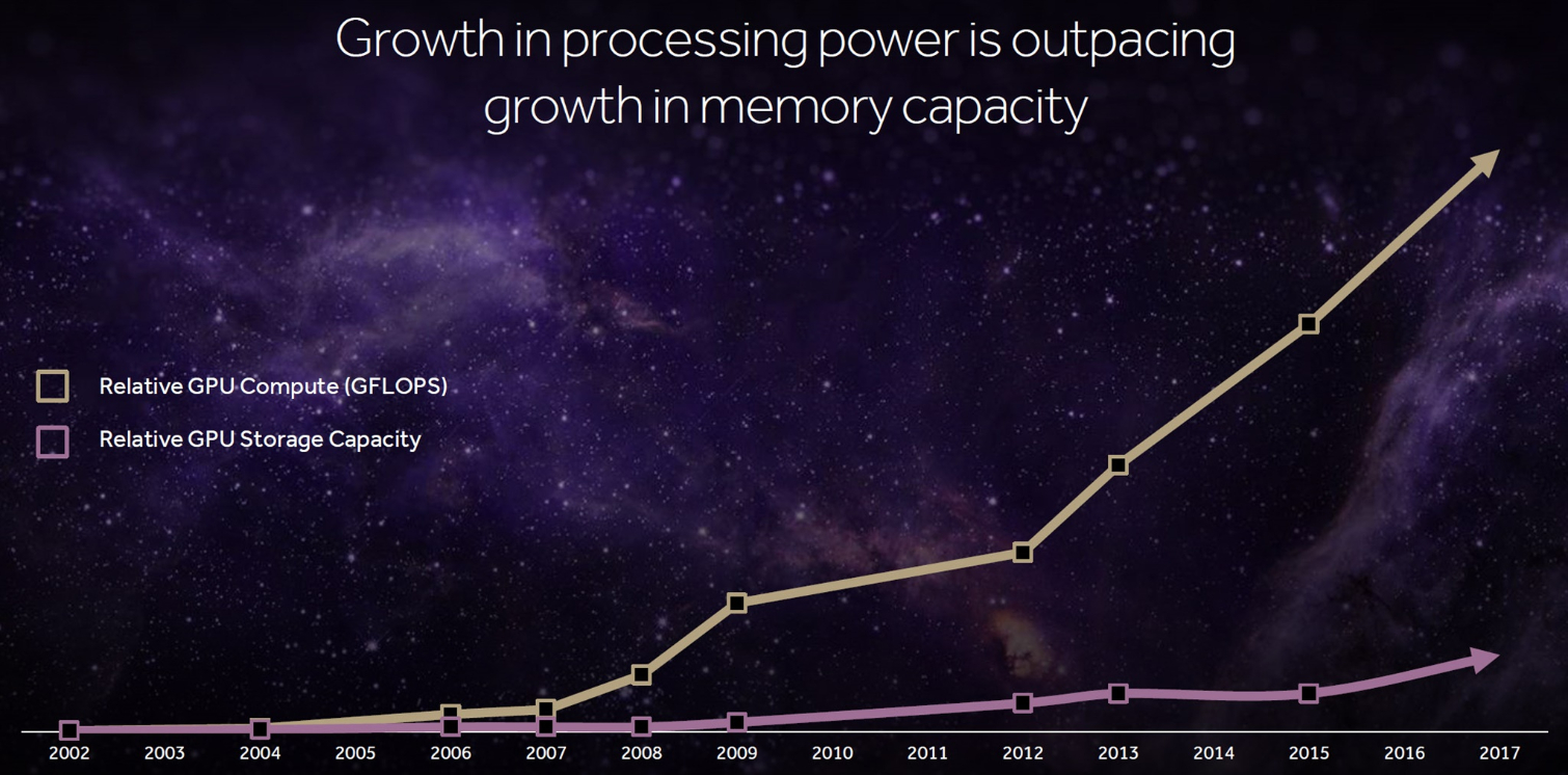
As a lead-in to Vega’s first architectural upgrade, Koduri presented slides showing the rapidly increasing sizes of game installs on desktop PCs, petabyte-class professional graphics workloads, and exabyte-plus training set sizes applicable to machine learning. He also mapped the growth of compute performance versus memory capacity.
Both AMD and Nvidia are working on ways to reduce host processor overhead, maximize throughput to feed the GPU, and circumvent existing bottlenecks—particularly those that surface in the face of voluminous datasets. Getting more capacity closer to the GPU in a fairly cost-effective manner seemed to be the Radeon Pro SSG’s purpose. And Vega appears to take this mission a step further with a more flexible memory hierarchy.
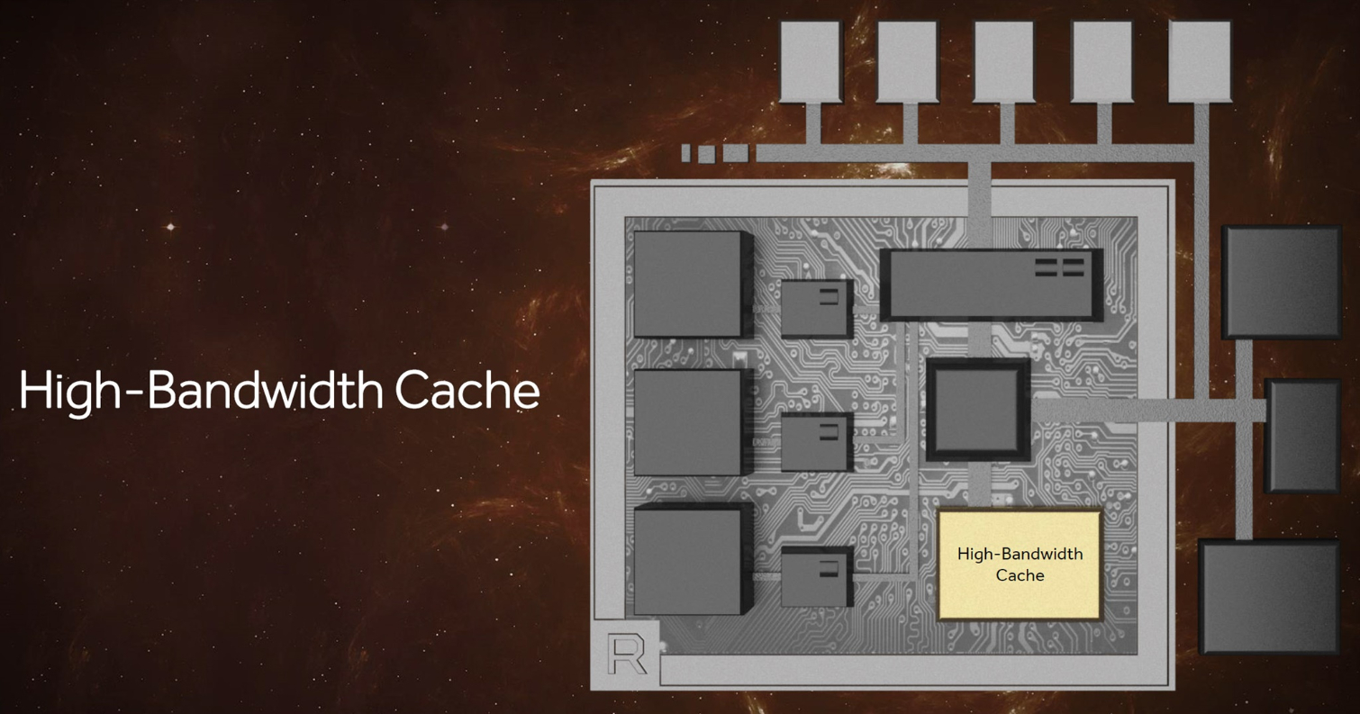
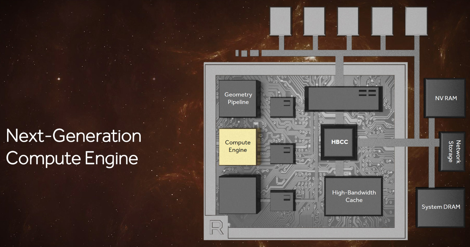
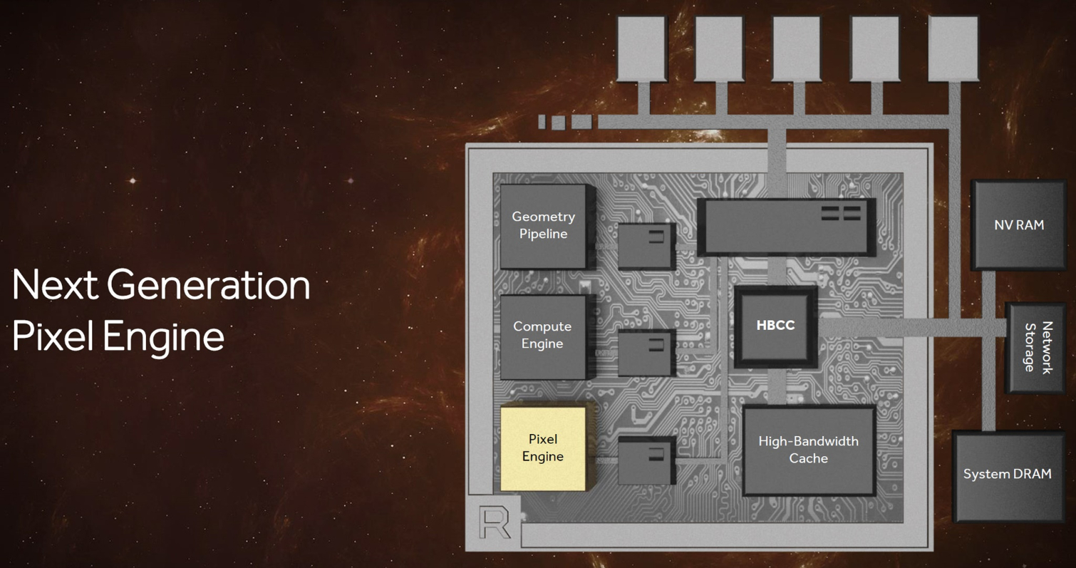
It’s no secret that Vega makes use of HBM 2; that information was on roadmaps through 2016. But we now know that AMD wants to call this pool of on-package memory—previously the frame buffer—a high-bandwidth cache. Got it? HBM2 equals high-bandwidth cache now. Why? Because AMD says so.
Get Tom's Hardware's best news and in-depth reviews, straight to your inbox.
No really, why? Well, according to Joe Macri, corporate fellow and product CTO, the vision for HBM was to have it be the highest-performance memory closest to the GPU. However, he also wanted system memory and storage available to the graphics processor, as well. In the context of this broader memory hierarchy, sure, it’s logical to envision HBM2 as a high-bandwidth cache relative to slower technologies. But for the sake of disambiguation, we’re going to continue calling HBM2 what it is.
After all, HBM2 in and of itself represents a significant step forward. An up-to-8x capacity increase per vertical stack, compared to first-gen HBM, addresses questions enthusiasts raised about Radeon R9 Fury X’s longevity. Further, a doubling of bandwidth per pin significantly increases potential throughput. If AMD uses the same 4-hi (four HBM dies) stacks of 700 MHz HBM2 that Nvidia introduced with the Tesla P100 accelerators last year, it would have a 16GB card pushing up to 720GB/s. There’s room for more capacity and bandwidth from there.
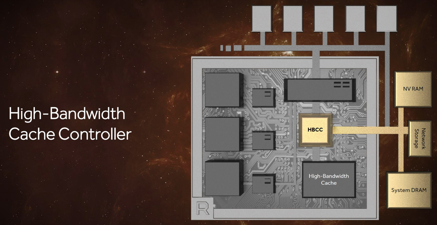
That’s the change we expect to have the largest impact on gamers as far as Vega's memory subsystem goes. However, AMD also gives the high-bandwidth cache controller (no longer just the memory controller) access to a massive 512TB virtual address space for those large datasets Raja discussed early in his presentation. Clearly, there’s some overlap between this discussion and the Radeon Instinct lineup AMD announced back in December.
We came away from this presentation with plenty of questions about how the Vega architecture’s broader memory hierarchy will be utilized, but Scott Wasson, senior product marketing manager at AMD, helped add clarity to the discussion by describing some of what the high-bandwidth cache controller can do. According to Wasson, Vega can move memory pages in fine-grained fashion using multiple, programmable techniques. It can receive a request to bring in data and then retrieve it through a DMA transfer while the GPU switches to another thread and continues work without stalling. The controller can go get data on demand but also bring it back in predictively. Information in the HBM can be replicated in system memory like an inclusive cache, or the HBCC can maintain just one copy to save space. All of this is managed in hardware, so it’s expected to be quick and low-overhead.
A New Programmable Geometry Pipeline
The Hawaii GPU (Radeon R9 290X) incorporated some notable improvements over Tahiti (Radeon HD 7970), one of which was a beefier front end with four geometry engines instead of two. The more recent Fiji GPU (Radeon R9 Fury X) maintained that same four-way Shader Engine configuration. However, because it also rolled in goodness from AMD’s third-gen GCN architecture, there were some gains in tessellation throughput, as well. Most recently, the Ellesmere GPU (Radeon RX 480) implemented a handful of techniques for again getting more from a four-engine arrangement, including a filtering algorithm/primitive discard accelerator.
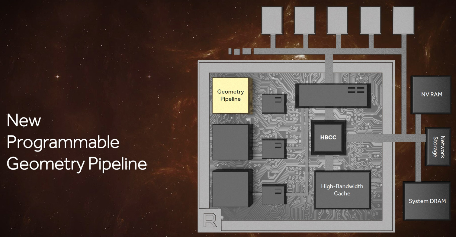
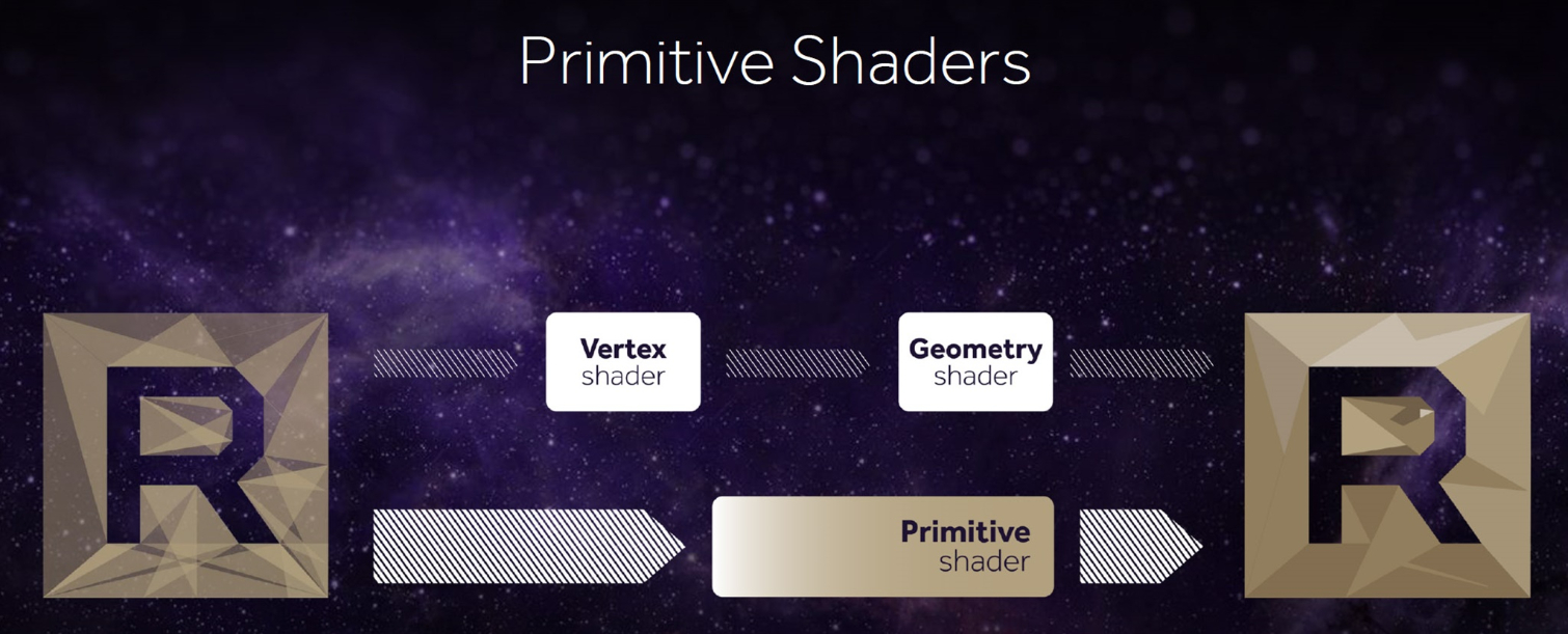
AMD’s backup slides tell us that Vega’s peak geometry throughput is 11 polygons per clock, up from the preceding generations' four, yielding up to a 2.75x boost. That specification comes from using a new primitive shader stage being added to the geometry pipeline. Instead of using the fixed-function hardware, this primitive shader uses the shader array for its work.
Mike Mantor, AMD corporate fellow, described this as having similar access as a compute shader for processing geometry in that it’s lightweight and programmable, with the ability to discard primitives at a high rate. AMD’s Wasson clarified further that the primitive shader’s functionality includes a lot of what the DirectX vertex, hull, domain, and geometry shader stages can do but is more flexible about the context it carries and the order in which work is completed.
The front-end also benefits from an improved workgroup distributor, responsible for load balancing across programmable hardware. AMD said this comes from its collaboration with efficiency-sensitive console developers, and that effort is now going to benefit PC gamers, as well.
The Vega NCU (Next-Generation Compute Unit)
Using its many Pascal-based GPUs, Nvidia is surgical about segmentation. The largest and most expensive GP100 processor offers a peak FP32 rate of 10.6 TFLOPS (if you use the peak GPU Boost frequency). A 1:2 ratio of FP64 cores yields a double-precision rate of 5.3 TFLOPS, and support for half-precision compute/storage enables up to 21.2 TFLOPS. The more consumer-oriented GP102 and GP104 processors naturally offer full-performance FP32 but deliberately handicap FP64 and FP16 rates so you can’t get away with using cheaper cards for scientific or training datasets.
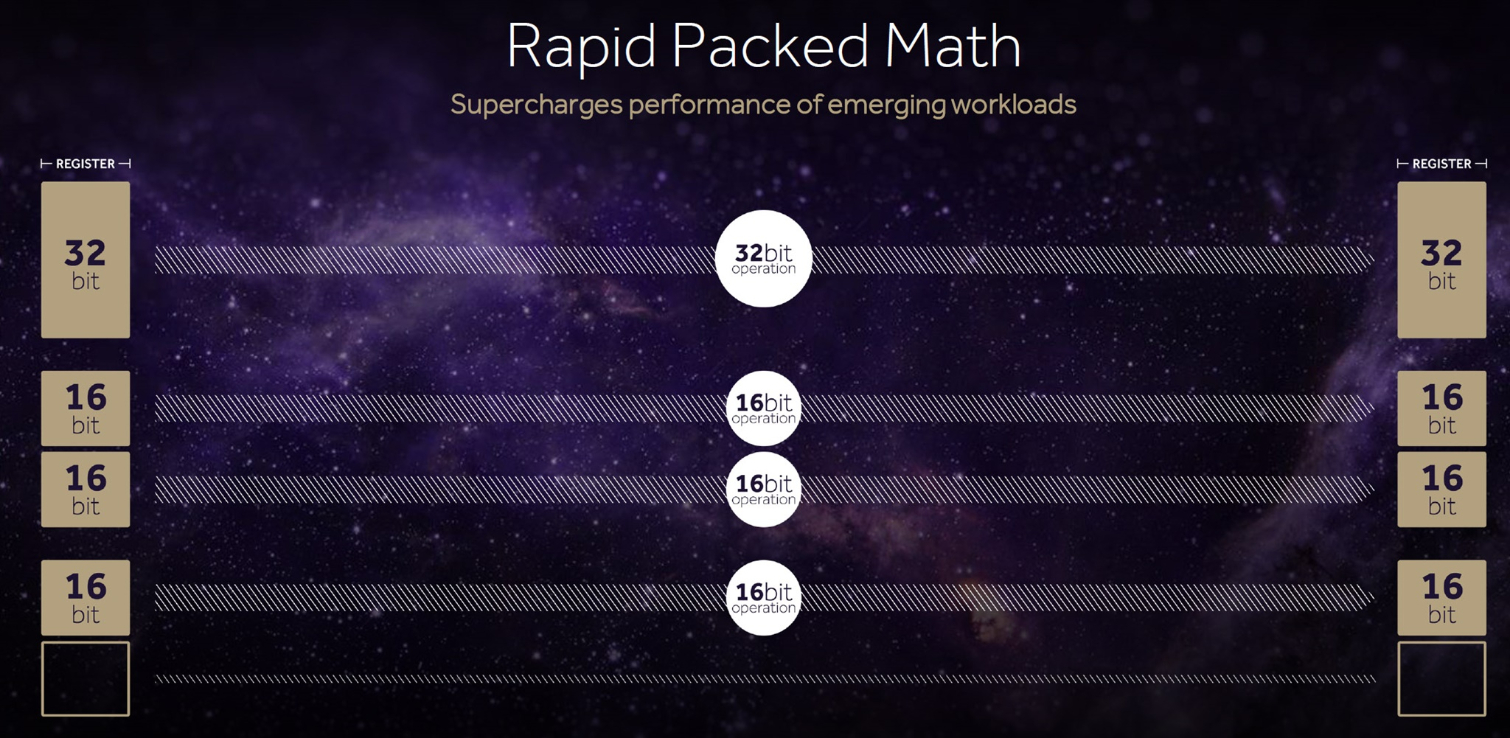
AMD, on the other hand, looks like it’s trying to give more to everyone. The Compute Unit building block, with 64 IEEE 754-2008-compliant shaders, persists, only now it’s being called an NCU, or Next-Generation Compute Unit, reflecting support for new data types. Of course, with 64 shaders and a peak of two floating-point operations/cycle, you end up with a maximum of 128 32-bit ops per clock. Using packed FP16 math, that number turns into 256 16-bit ops per clock. AMD even claimed it can do up to 512 eight-bit ops per clock. Double-precision is a different animal—AMD doesn’t seem to have a problem admitting it sets FP64 rates based on target market.
The impetus for this flexibility may have very well come from the console world. After all, we know Sony’s PlayStation 4 Pro can use half-precision to achieve up to 8.4 TFLOPS—twice its performance using 32-bit operations. Or perhaps it started with AMD’s aspirations in the machine learning space, resulting in products like the upcoming Radeon Instinct MI25 that aim to chip away at Nvidia’s market share. Either way, consoles, datacenters, and PC gamers alike stand to benefit.
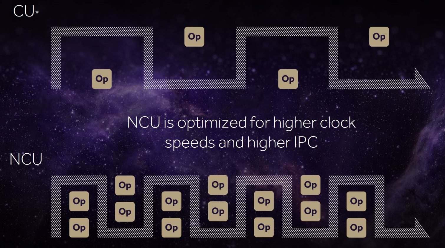
AMD claimed the NCUs are optimized for higher clock rates, which isn’t particularly surprising, but it also implemented larger instruction buffers to keep the compute units busy.
A Next-Generation Pixel Engine
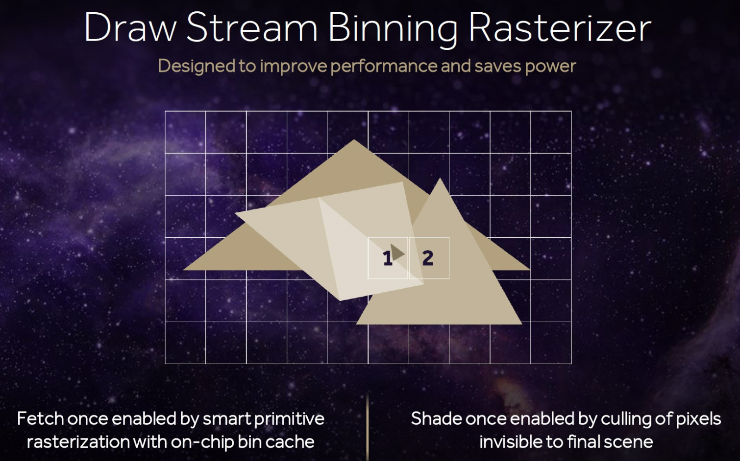
The fourth topic of AMD’s early Vega disclosures is actually a two-parter. First up is the draw stream binning rasterizer, attached to the traditional rasterization hardware, which Koduri said is able to improve performance and save power. At a high level, an on-chip bin cache allows the rasterizer to fetch data only once for overlapping primitives, and then shade pixels only once by culling pixels not visible in the final scene.
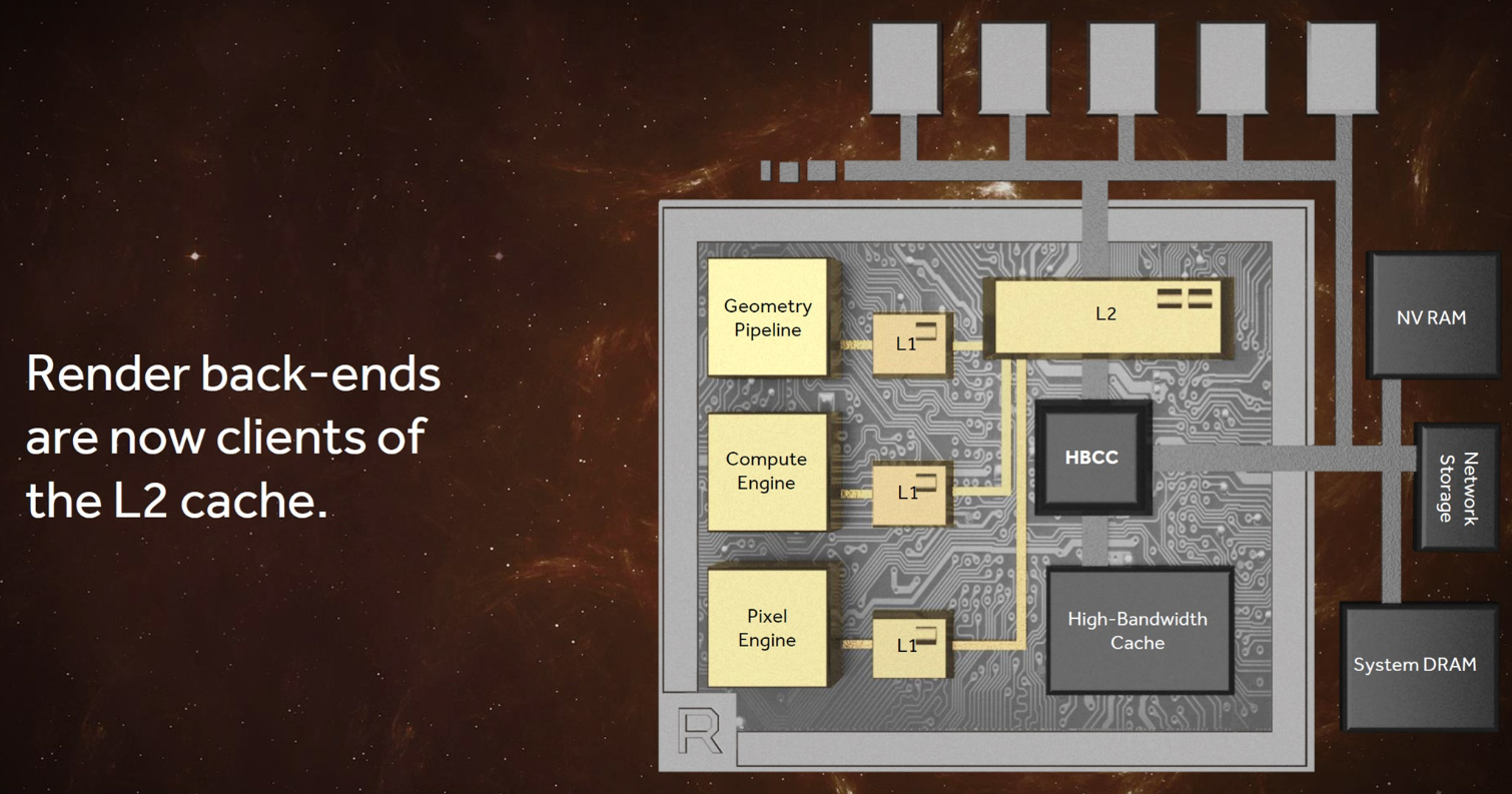
Second, AMD is fundamentally changing its cache hierarchy by making the render back-ends clients of the L2. In architectures before Vega, AMD had non-coherent pixel and texture memory access, meaning there was no shared point for each pipeline stage to synchronize. In the example of texture baking, where a scene is rendered to a texture for reuse later and then accessed again through the shader array, data has to be pulled all the way back through off-die memory. Now, the architecture has coherent access, which AMD said particularly boosts performance in applications that use deferred shading.
Although much of what Koduri presented requires development effort on the software side to utilize, he still wrapped his slide deck with a demo of Doom running at 4K under its most taxing detail settings on an early Vega board in the 70+ FPS range. Based on the numbers we were seeing in our Titan X review, that’s somewhere in between a GTX 1080 and Titan X.
As AMD's driver team gets its feet wet with Vega, we expect to see those performance numbers increase. We just hope it doesn't take the company another six months to feel comfortable giving us the full story. By then, its principal competition will be over a year old.
-
I bet it performs <= 1080 meaning Nvidia makes much more efficient GPUs, GPU which overclocked to 2025Mhz with evga air type cooler doesn't go over 62C. I would not be surprised if Nvidia releases 1080ti to spoil it for AMD. Regardless of this, it is good we are getting competition CPU/GPU market, now let's make everyone lower their prices.Reply
-
ammaross You guys seem to have missed the RX490 slide in the pre-roll that said 05/01/2017....Reply -
bloodroses Reply19109696 said:I bet it performs <= 1080 meaning Nvidia makes much more efficient GPUs, GPU which overclocked to 2025Mhz with evga air type cooler doesn't go over 62C. I would not be surprised if Nvidia releases 1080ti to spoil it for AMD. Regardless of this, it is good we are getting competition CPU/GPU market, now let's make everyone lower their prices.
I'm guessing you didn't read the end of the article:
"Although much of what Koduri presented requires development effort on the software side to utilize, he still wrapped his slide deck with a demo of Doom running at 4K under its most taxing detail settings on an early Vega board in the 70+ FPS range. Based on the numbers we were seeing in our Titan X review, that’s somewhere in between a GTX 1080 and Titan X.
As AMD's driver team gets its feet wet with Vega, we expect to see those performance numbers increase."
So figure between 1080 and titan performance. It's the same thing that happened last generation until Nvidia dropped the 980ti bomb to spoil the parade on AMD's Fury X. I bet a lot of Titan owners were furious when that happened as well. The 1080ti more than likely will be the same way. -
dusty13 Reply19109696 said:I bet it performs <= 1080 meaning Nvidia makes much more efficient GPUs, GPU which overclocked to 2025Mhz with evga air type cooler doesn't go over 62C. I would not be surprised if Nvidia releases 1080ti to spoil it for AMD. Regardless of this, it is good we are getting competition CPU/GPU market, now let's make everyone lower their prices.
I very much doubt that. AMDs main issue in the past years was drivers and efficiency both of which they finally seem to get better at.
when it comes to silicon amd actually always did have very powerful gpus sitting around but they took ages to get the drivers right. that's why they are perceived slower by so many people who just read one of those reviews that keep on showing the performance data from launch day. NVidia does a much better job getting performance right out of the gate (especially with dx11), amds driver team seems to be drunk half the time and needs about 6-9 months to actually get decent drivers done (at least this was the case for the last few years, can't check now as I do not have an amd card at the moment).
if you look up reviews of cards that actually retest the performance repeatedly, the amd cards usually catch up or even surpass the NVidia counterparts in time but at that point no one notices anymore and so the mindshare is firmly with NVidia being faster.
when it comes to efficiency amd finally made some progress with the rx4xx cards. they are not equal yet but they are close enough to NVidia again. if vega is as efficient or an upgrade to the rx4xx series power draw is a non-argument for either side.
NVidia on the other hand seems to have issues getting any substantial gains out of DX12 compared to DX11. since their driver team is superb in my experience this seems to be a design limitation in the chip, so unless they revamp pascal or come up with something completely new within the next 6 months amd has more than a small chance to beat the 1080(ti) with vega if it pans out half as good as the leaks suggest at the moment.
And yes, I too am looking forward very much to an actual alternative to overpriced NVidia highend cards - amd being competitive in high end again will bring down the ridiculous prices quite a bit if nothing else and that is a very good thing. -
kiniku At least Ryzen had a hand picked benchmark. But in the case of Vega we have a video with a drummer using one drumstick telling us to "join the revolution". The overhyped followup today is tons of new ambiguous, pseudo-scientific, terms. I really had been thinking of my next build going Ryzen/Vega. I'm having second thoughts now.Reply -
fynxer VEGA in Q2 is to late. nVidia cancelled 1080Ti and will now steam full speed ahead to release VOLTA just in time to overshadow VEGAs arrival to market. Once again AMDs drags its feet, if they where to release VEGA in January they would have been ahead with a fighting chance but now they will give nVidia just the amount of time it needs to counter VEGA in full force with VOLTA in Q2.Reply -
redgarl We can expect Vega flag ship to be as strong as the 1080 TI, it's going to be released at about the same time so price will be important.Reply
However, the 1080 GTX is a bad card design and I don't believe the TI is going to be any better. It's the first time in my life that a card literally explode in front of me. Nvidia, the way it meant to be... sure... -
Zareek 5/1/17 is too late! AMD is massively missing their release target dates. Let's hope they don't miss their performance targets too!Reply -
kwc813 It's only logical putting your fastest memory next to the GPU/CPU. It's always been a given that potential speed increases are derived from the capacity of the data bus. What I see here is an attempt to address throughput, and THAT'S exciting...almost as exciting as seeing a valid competitor even challenge Nvidia in performance at the only race most people know anything about..FPS.Reply
What AMD is doing can only benefit the consumer in general, NOT just the gamer. When you get into talking publicly about peta-scale data movement place to place then you're serious...might be time to invest in AMD/Radeon stock if they get their heads out quick enough this time!!! Even if they don't everyone knows there's effort being made, and you've always gotta be smarter coming from behind than you have to be when you're number 1. This could be fun!
.
