APC BX1000 Click-of-Death Repair
What Is A Charge Pump?
When I found the choppy op-amp supply, the first question I asked myself was: where is it coming from? At first, I thought there may have been some fancy reuse of the switching supply’s circuit. But upon further inspection, there are no extra taps on the secondary winding and no extra diodes to accommodate that. As additional confirmation, I compared the switching frequency of the switching supply with the LM358 supply’s chopping and found that they were in completely different ranges: 120kHz for the 24V supply versus 2kHz for the LM358. Where could that 2kHz be coming from? The micro-controller. After some more poking around, I found a controller pin with a 2kHz square wave on it. What sort of common power supply topology operates from a computer-driven clock? A charge pump.
Charge pumps offer a simple, convenient, inexpensive, and also inefficient (25% at best) way of generating low-power (typically no more than a few milliamps) supply rails, where it makes no sense to bother with the cost and complexity of magnetic switching regulators. Their basic implementation requires little more than diodes, capacitors, and some form of clock source. They are frequently used in applications like generating negative rails for op-amps and sensors. In some cases, much of the work is done by using a pair of micro-controller output pins, driving one pin alternately high/low and the other low/open. When higher-output voltages than what the micro-controller can handle on its I/O pins are needed, a CPU-driven charge pump may use some form of level-shifting circuitry to power the charge pump from a higher voltage supply.
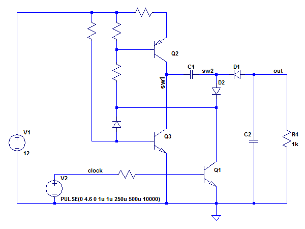
I have not attempted to reverse-engineer the BX1000’s circuit, but based on the number of resistors, transistors, and diodes conspicuously laid out in the LM358’s immediate neighborhood, I suspect it is similar to the circuit I have drawn. When the ‘clock’ is high, Q1 and Q2 get turned on, charging C1 positive on the ‘SW1’ side. When ‘clock’ goes low, Q1 and Q2 turn off, Q3 gets turned on by its bias resistor and connects the positively-charged SW1 side of C1 to ground, causing its negative voltage to appear at SW2, which in turn forward-biases D1 and causes negative voltage to appear at the output. The circuit may look a little complicated, but between that and driving a magnetic circuit, this is much simpler and cheaper. As a bonus, the output voltage in this configuration cannot exceed the input voltage minus diode voltage drops, which means there is no need for a feedback circuit to prevent excessive output voltage. Since there are only two transistors in APC’s circuit, Q1 on my schematic could be substituted for an open-collector output on the micro-controller.
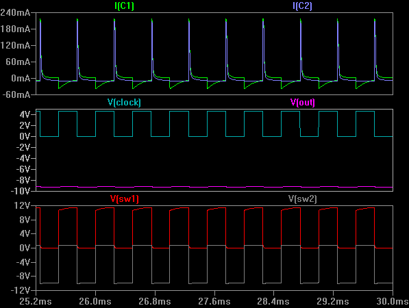
What sort of waveforms do you get out of a charge pump? Here are the most important ones: the input clock, output voltage, voltage on both sides of the transfer capacitor (SW1 and SW2), and current through the two capacitors. As you can see, as voltage at SW1 switches between 0V and 12V, voltage at SW2 switches between -10V and 0V with slight peaks on the output matching negative peaks at SW2. The more interesting part is the capacitor current waveform: dumping charge into capacitors produces some large current peaks, and these waveforms show about 40 mARMS going through C1 and C2 respectively. Sounds tiny? Yes it does. Then again, you have to keep in mind that these are small electrolytic capacitors and general-purpose capacitors of this size are often only rated for 30-50 mARMS of ripple. With no manufacturer logo on the capacitor and “H13” failing to yield a distinctive match, I have no idea what the capacitor’s specifications are supposed to be. So assuming the worst, it looks like C41 may have died from a decade of being run at close to its ripple current rating.
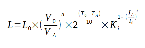
What was that capacitor lifespan estimation equation again? Assuming a typical rated lifespan of 2000 hours for L0 at a rated temperature of 105°C for T0 and a pessimistic 35mARMS for the ripple rating I0 for the specifications' unknowns, an average value of 1.5 for n and a similarly typical value of 4 for Ki for the manufacturer’s reliability model unknowns, an operating temperature of 50°C for TA, ripple current of 40mARMS for IA, and applied voltage of 12V for VA, I get an estimated lifespan of just over ninety thousand hours. If my guesses are reasonably accurate, then it appears that the capacitor failed on cue with frightening accuracy.
The other possibility is that a proper low-ESR capacitor was used, which would have had a ripple rating in the hundreds of milliamps. In that case, the Ki term would have catapulted the projected lifespan sky-high and the only explanation for the failure would be a latent manufacturing or handling defect that slowly evolved into a break between either terminal and the aluminum foils.
Which one do you think is most likely? Unless I find the specifications, both seem equally plausible.
Get Tom's Hardware's best news and in-depth reviews, straight to your inbox.
MORE: APC BR1000G Tear-Down
MORE: APC BN650M1-CA Tear-Down
MORE: APC BGE90M-CA Tear-Down
Current page: What Is A Charge Pump?
Prev Page From Input To Output Next Page Capacitors: Can’t Live With ‘Em, Can’t Live Without ‘Em-
Zaxx420 'Now on to the next one: why did the capacitor fail in the first place?'Reply
That's one aspect that sooo many folks never consider or can't be bothered to investigate. Just like a fuse that keeps blowing...there is something that's causing it to blow...even if it lasts a while before blowing. Even worse is when they decide to bridge it with a piece of wire or wrap the blown (glass) fuse with aluminum foil. Now I'm guilty as well but ONLY long enuff to get myself out of a jam...like being stranded on the side of the road or something. Just never do it with a high current load or if it's blowing the instant you turn it on...and never with a sensitive/expensive critical component like the ignition ECU of your self semi-restored muscle car project...don't ask. -
Daniel Sauvageau Reply
The repair is already done and I'm not set up for recording - don't even own a video camera or webcam. Even if I did own one, I'm no good with talking and working at the same time. Also, if I posted repairs on YouTube, I wouldn't be able to post them on THG since THG is paying me for exclusive publication.18828366 said:When you do fix it, can you YouTube it?
Too much credit :) This is basic troubleshooting, anyone going through electronics tech training should be able to do as before graduation.18830162 said:You are so smart.
-
jcamilo70 I have a 2005 RS1200 that died on me, making clicking sound constantly, and only turning on directly into battery mode.Reply
Where did you manage to get the replacement pieces? Where could I find the micro-controller for this unit or how should I identify its part number in order to look for it? -
Daniel Sauvageau Reply
The only part I needed to replace here was that single capacitor. Where did I get the capacitor from? It was just one of many leftover parts I've accumulated either from ordering more parts than necessary for past repairs/projects, or parts I had ordered for potential future projects to pad orders for free S&H. I may have over $2000 worth of parts in my spare parts and samples boxes.18830308 said:I have a 2005 RS1200 that died on me, making clicking sound constantly, and only turning on directly into battery mode.
Where did you manage to get the replacement pieces? Where could I find the micro-controller for this unit or how should I identify its part number in order to look for it?
For the micro-controller, I didn't touch it. Even if I had wanted to replace it, they can only be ordered blank from parts distributors (or pre-programmed with your own firmware for large enough orders or distributors that offer such a service for an additional fee) and those would be no good without the correct firmware to put on them. If the controller died, it is game over unless you can find a donor UPS based on the same PCB. -
powernod This example showed us the importance of high quality caps to be used in such critical components such as a UPS/PSU. A single cap-failure (*from the many a UPS uses) and caused total malfunction of the UPS !!Reply
P.S. This review has also shown us the importance/need for UPSs reviews. Since PSUs are being thoroughly reviewed for many years, i don't understand why UPSs shouldn't be reviewed as well!! A PSU's proper operation is in consequence with the proper operation of the hardware that "feeds" a PSU (*UPS)
P.S.2 : Great article by the way!!


