NVIDIA GeForceFX: Brute Force Attack Against the King
Get Tom's Hardware's best news and in-depth reviews, straight to your inbox.
You are now subscribed
Your newsletter sign-up was successful
The GeForceFX GPU, Continued
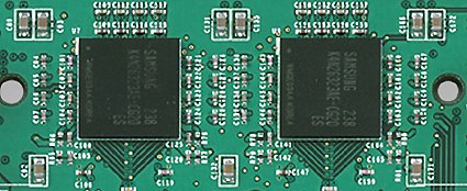
DDR-II memory is completely new to graphics cards, and the GeForceFX GPU was designed for it. The new memory modules allow for much faster data rates than DDR modules have offered up to now. With DDR-II, as with DDR, data is transferred on both flanks of the signals, which means two transfers per clock cycle and not four, as you might expect. The difference lies in the structure of the memory cells - instead of transferring in bursts of 2, DDR-II internally transfers in bursts of four. This allows it to run the RAM at significantly higher clock speeds, because the clock rates within the memory module have been halved compared to DDR. With DDR-II, the data is doubled within the memory cell and not during the transfer. However, the GPU has to be adapted to this, since data is now transferred in bursts of four instead of two, as was the case with DDR.
The memory bandwidth of the GeForceFX is therefore calculated exactly as it is with the usual DDR memory:
128 bits / 8 bits/Byte * 500 MHz * 2 (2 transfers/clock) = 16.0 GB/sec
Article continues belowThe memory bandwidth, however, is a point of criticism with the GeForceFX. 16 GB/s is much less than the 19.8 GB/s from its competitor, the ATI Radeon 9700 PRO. ATI utilizes typical DDR memory with moderate clock speeds, and instead increases the bus width from 128 bit to 256 bit in order to raise the bandwidth. NVIDIA leaves it at 128 bit and clocks the memory faster, using DDR-II, of course.
In order to compensate for the apparent disadvantage with memory bandwidth, NVIDIA equipped the chip with Color Compression, in addition to Z-Compression. This enables loss-free compression of color data with a factor of 4:1 in real time. According to NVIDIA, this compression of color data is very effective, since even the color data on the polygon edges can be perfectly compressed.
A last new feature to mention is AGP 8x, which, despite its ability to double data transferred from the CPU to the card, does not have much of an impact in practice. However, games to come, which are designed to take advantage of this greater bandwidth, should definitely give gamers the extra power they would expect from AGP 8x.
An overview of the chip:
Get Tom's Hardware's best news and in-depth reviews, straight to your inbox.
- Produced on a 0.13µ process
- Flip-chip design
- 256 bit GPU
- 125 million transistors
- Eight Pixel Shaders
- Vertex Shader Array
- Clock speeds of at least 500 MHz
- DDR-II memory starting at 500 MHz (1 GHz DDR)
- 128 bit memory bus
- Optimized memory interface with lossless Z-compression and color data compression * * AGP 8X
- FX Flow - proprietary copper heat pipe cooling solution
Current page: The GeForceFX GPU, Continued
Prev Page The GeForceFX GPU, Continued Next Page The Card