P67 Motherboard Roundup: Nine $150-200 Boards
Improved per-clock performance and higher achievable frequencies are sure to put Intel’s latest K-Series CPUs on top of many builders’ whish lists, but they’ll still need a new socket to put it in. We test nine enthusiast-oriented LGA-1155 motherboards.
Overclocking Results
| BIOS Frequency and Voltage settings (for overclocking) | |||
|---|---|---|---|
| Row 0 - Cell 0 | ASRock P67 Extreme4 | Asus P8P67 Pro | Biostar TP67XE |
| CPU Base Clock | 95-110 MHz (1 MHz) | 80-300 MHz (0.1MHz) | 100-300 MHz (0.1MHz) |
| CPU Multiplier | Up to 57x | Up to 57x | Up to 100x* |
| DRAM Data Rates | 1066-2133 (266.6 MHz) | 800-2400* (266.6 MHz) | 1066-2133 (266.6 MHz) |
| CPU Vcore | 0.86-1.52V (5 mV) | 0.80-1.99V (5 mV) | 1.00-1.79V (10 mV) |
| Sys. Agent Voltage | 0.66-1.87 (12.5 mV) | 0.80-1.70V (6.25 mV) | 0.90-1.61V (12.5 mV) |
| PCH Voltage | 0.78-1.65V (9 mV) | 0.80-1.70V (10 mV) | 1.00-1.50V (12.5 mV) |
| DRAM Voltage | 1.20-1.80V (15 mV) | 1.20-2.20V (6.25 mV) | 1.30-2.20V (12.5 mV) |
| CAS Latency | 5-15 Cycles | 3-15 Cycles | 3-15 Cycles |
| tRCD | 4-15 Cycles | 4-15 Cycles | 3-15 Cycles |
| tRP | 4-15 Cycles | 4-15 Cycles | 3-15 Cycles |
| tRAS | 10-40 Cycles | 4-40 Cycles | 9-63 Cycles |
| BIOS Frequency and Voltage settings (for overclocking) | |||
|---|---|---|---|
| Row 0 - Cell 0 | ECS P67H2-A2 | Foxconn P67A-S | Gigabyte P67A-UD4 |
| CPU Base Clock | 100-106 MHz (0.16 MHz) | 100-300 MHz (0.1 MHz) | 80-200 MHz (0.1 MHz) |
| CPU Multiplier | Up to 50x | Up to 50x | Up to 57x |
| DRAM Data Rates | 1066-2133 (266.6 MHz) | 1066-2133 (266.6 MHz) | 1066-2133 (266.6 MHz) |
| CPU Vcore | -0.8 to +0.63V (50 mV) | +1.0V (20 mV) | 0.75-1.70V (50 mV) |
| Sys. Agent Voltage | -0.8 to +0.63V (50 mV) | Not Adjustable | 0.66-1.31V (10 mV) |
| PCH Voltage | 1.08-1.23V (50 mV) | Not Adjustable | 0.84-1.94V (20 mV) |
| DRAM Voltage | -0.8 to +0.63V (50 mV) | 1.50-2.00V (12.5 mV) | 0.90-2.60V (20 mV) |
| CAS Latency | 3-15 Cycles | 3-15 Cycles | 5-15 Cycles |
| tRCD | 3-15 Cycles | 3-15 Cycles | 1-15 Cycles |
| tRP | 3-15 Cycles | 3-15 Cycles | 1-15 Cycles |
| tRAS | 9-63 Cycles | 9-63 Cycles | 1-40 Cycles |
| BIOS Frequency and Voltage settings (for overclocking) | |||
|---|---|---|---|
| Row 0 - Cell 0 | Intel DP67BG | Jetway HI08 | MSI P67A-GD65 |
| CPU Base Clock | 100-120 MHz (1 MHz) | 100-300 MHz (0.1 MHz) | 89-282 MHz (0.06 MHz) |
| CPU Multiplier | Up to 57x | Up to 50x | Up to 60x* |
| DRAM Data Rates | 1066-2133 (266.6 MHz) | 1066-2133 (266.6 MHz) | 800-2133 (266.6 MHz) |
| CPU Vcore | 1.00-2.30V (6.25 mV) | +0.255V (1 mV) | 0.80-1.80V (5 mV) |
| Sys. Agent Voltage | 0.85-1.75V (25 mV) | 1.14-1.25V (35 mV) | 0.93-1.59V (20 mV) |
| PCH Voltage | 1.00-1.50V (6.25 mV) | 1.08-1.18V (34 mV) | Not Adjustable |
| DRAM Voltage | 1.20-2.00V (10 mV) | 1.54-2.20V (50 mV) | 1.11-2.46V (6.25 mV) |
| CAS Latency | 5-16 Cycles | 5-16 Cycles | 5-15 Cycles |
| tRCD | 5-16 Cycles | 5-16 Cycles | 4-15 Cycles |
| tRP | 5-16 Cycles | 5-16 Cycles | 4-15 Cycles |
| tRAS | 15-75 Cycles | 15-75 Cycles | 10-40 Cycles |
*indicates a setting that exceeds available CPU ratios
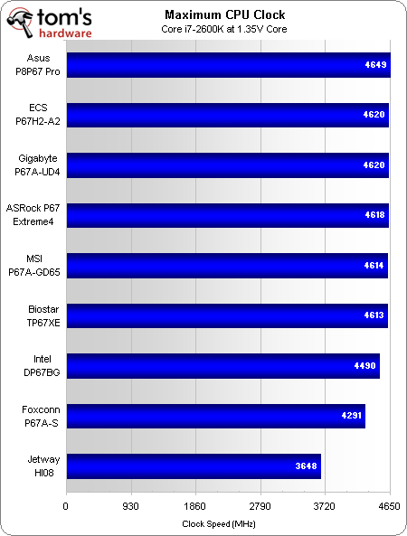
We probably don’t need to remind anyone that Intel’s K-series processors are required to get anything greater than a nominal overclock from its LGA 1155 platform, since its base clock is almost stuck. Even then, overclocking is done by manipulating Turbo Boost multipliers. Asus still manages to edge out its competitors in CPU overclocking, while the HI08’s broken Turbo Boost forces it to rely on that narrow BCLK capability.
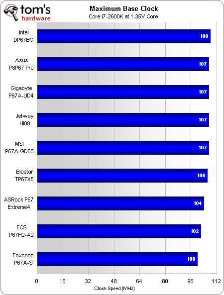
Intel breaks past BCLK expectations, but only because we tested this capability with the CPU at its stock multiplier. Higher stress that occurs at higher multipliers generally tends to make BCLK increases more difficult, so we’ll leave the combination of BCLK and high multipliers to the world of competitive overclocking.
Before we move on, we must also note that increased BCLK has a habit of corrupting drives, since higher clocks affect PCI Express and DMI. Our tests focused on CPU, GPU, and DRAM stability, since data corruption can take days to rear its ugly head.
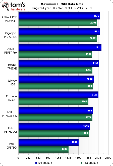
The same BCLK limitations that affect CPU overclocking also limit RAM. Jetway’s HI08, for example, had boot issues when using its 21.33x memory multiplier, forcing us to push its BCLK limits to find a memory speed that’s likely short of the motherboard’s actual capability. Intel’s DP67BG was also capable of running beyond DDR3-2133, but we couldn’t force a cold boot at anything above the charted settings.
Get Tom's Hardware's best news and in-depth reviews, straight to your inbox.
Current page: Overclocking Results
Prev Page Benchmark Results: Productivity Next Page Power, Heat, and Efficiency-
reprotected I thought that the ECS looked pretty sick, and it did perform alright. But unfortunately, it wasn't the best.Reply -
rantsky You guys rock! Thanks for the review!Reply
I'm just missing benchmarks like SATA/USB speeds etc. Please Tom's get those numbers for us! -
rmse17 Thanks for the prompt review of the boards! I would like to see any differences in quality of audio and networking components. For example, what chipsets are used for Audio in each board, how that affects sound quality. Same thing for network, which chipset is used for networking, and bandwidth benchmarks. If you guys make part 2 to the review, it would be nice to see those features, as I think that would be one more way these boards would differentiate themselves.Reply -
VVV850 Would have been good to know the bios version for the tested motherboards. Sorry if I double posted.Reply -
flabbergasted I'm going for the ASrock because I can use my socket 775 aftermarket cooler with it.Reply -
stasdm Do not see any board worth spending money on.Reply
1. SLI "support". Do not understand why end-user has to pay for mythical SLI "sertification" (all latest Intel chips support SLI by definition) and a SLI bridge coming with the board (at least 75% of end users would never need one). The bridge should come with NVIDIA cards (same as with AMD ones). Also, in x8/x8 PCIe configuration nearly all NVIDIA cards (exept for low-end ones) will loose at least 12% productivity - with top cards that is about $100 spent for nothing (AMD cards would not see that difference). So, If those cards are coming as SLI-"sertified" they have to be, in the worst case, equipped by NVIDIA NF200 chip (though, I would not recommend to by cards with this PCIe v.1.1 bridge). As even NVIDIA GF110 cards really need less than 1GB/s bandwidth (all other NVIDIA and AMD - less than 0.8GB/s)and secondary cards in SLI/CrossFire use no more than 1/4 of that, a normal PCIe v.2.0 switch (costing less than thrown away with x8/x8 SLI money) will nicely support three "Graphics only" x16 slots, fully-functional x8 slot and will provide bandwidth enough to support one PCIe v.2.0 x4 (or 4 x x1) slot(s)/device(s).
2. Do not understand the author euphoria of mass use of Marvell "SATA 6G" chips. The PCIe x1 chip might not be "SATA 6G" by definision, as it woud newer be able to provide more than 470GB/s (which is far from the standard 600GB/s) - so, I'd recommend to denote tham as 3G+ or 6G-. As it is shown in the upper section, there is enough bandwidth for real 6G solution (PCIe x8 LSISAS 2008 or x4 LSISAS 2004). Yes, will be a bit more expensive, but do not see the reason to have a palliative solutions on $200+ mobos.
-
I was hoping that the new Asus Sabertooth P67 would be included. Its new design really is leaving people wondering if the change is as good as they claim.Reply


