Nvidia Tegra K1 In-Depth: The Power Of An Xbox In A Mobile SoC?
Nvidia gave us an early look at its Tegra K1 SoC at its headquarters in Santa Clara. By far the most noteworthy change is a shift from programmable vertex and pixel shaders to the company's Kepler architecture, enabling exciting new graphics capabilities.
Tegra K1’s GPU: More Or Less One SMX
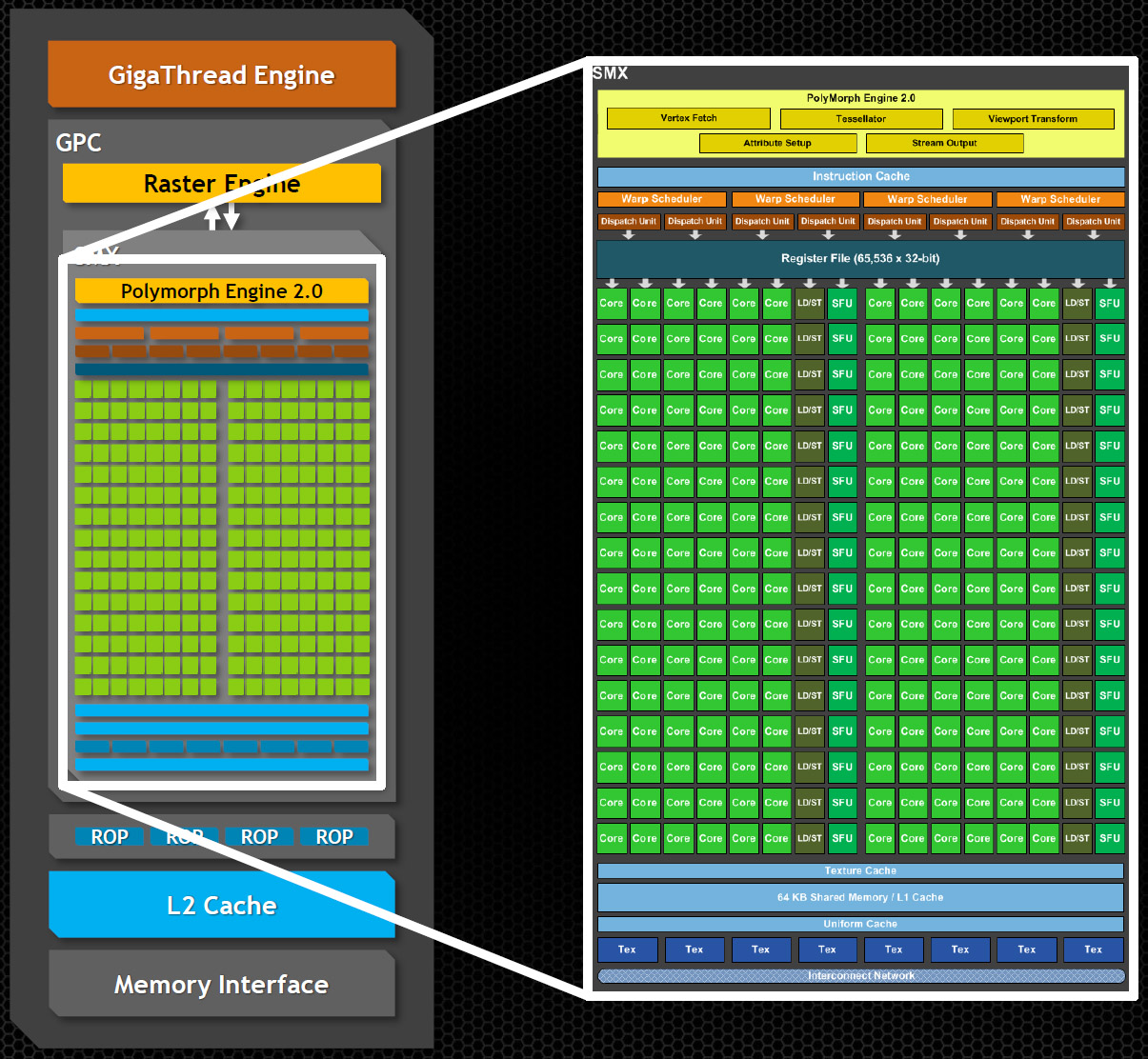
There will clearly be limitations to what Tegra K1 runs smoothly. Yes, it leverages the Kepler architecture. But the specific implementation is necessarily distilled in order to fit within a constrained power budget. In essence, we’re looking at one Streaming Multiprocessor built into a single Graphics Processing Cluster. The SMX contains 192 CUDA cores. Instead of 16 texture units, which is what you find on the desktop, Nvidia pares Tegra K1’s SMX down to eight. And whereas each ROP outputs eight pixels per clock in, say, GK104, Tegra K1 drops to four.
Although Nvidia didn't give us a specific clock rate for its graphics complex, one of its slides mentions a 365 GFLOPS peak shader performance figure. With 192 shaders, that'd put frequency right around 950 MHz.
Some of the other changes needed to enable Kepler on Tegra K1 are more difficult to illustrate. In short, if you look at the GPU block diagram, everything in grey, representing the fabric by which components of the engine communicate with each other, was replaced to optimize for efficiency. Although Nvidia constructed its next-generation Maxwell architecture with mobile in mind, you will continue to see the company utilize distinctly different fabrics to build its mobile and scaled-up GPUs, balancing performance and power consumption.
Article continues belowLearn About Nvidia's SMX
If you want to know more about Nvidia’s nomenclature and how its SMX appears in a discrete graphics architecture, check out GeForce GTX 680 2 GB Review: Kepler Sends Tahiti On Vacation.
Nvidia is quick to point out that it didn’t handicap certain other features of the architecture. For example, even though tessellation is exposed through DirectX 11 and OpenGL, the same second-gen PolyMorph engine found in desktop Kepler-based GPUs is still part of the SMX. This isn’t the first we’ve heard of DirectX 11-compliant tessellation enabled in hardware—Qualcomm’s Snapdragon 805 with Adreno 420 graphics is also equipped with hull, domain, and geometry shader support, as are Vivante’s licensable Vega cores. Nvidia is confident that its implementation is best, but there’s simply no way to test the company’s claims right now. We suspect, however, that industry-wide adoption of features like tessellation and geometry shading will make developers more likely to utilize those capabilities in next-gen games.
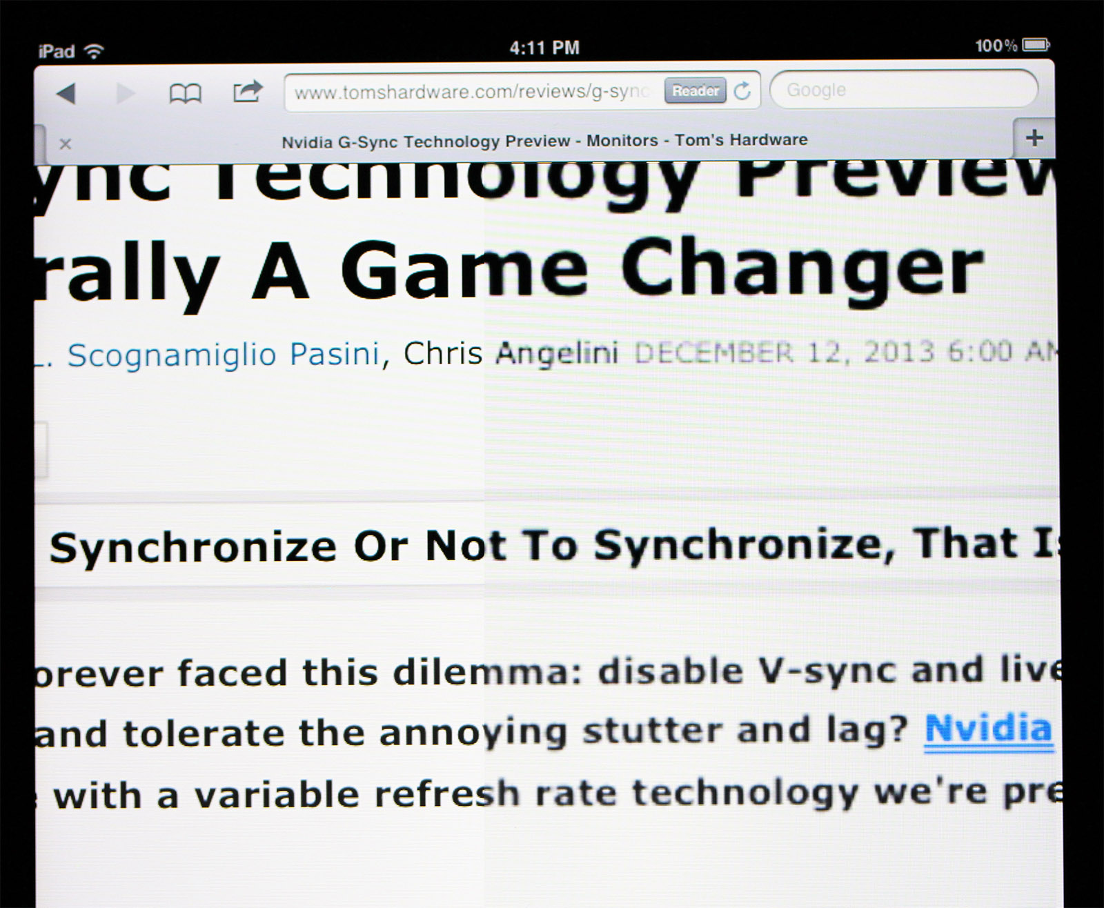
GPU-accelerated path rendering is another technology that Nvidia experimented with on its big GPUs first (back in 2001, in fact), and is now trying to advocate in the mobile world. Briefly, path rendering is involved in resolution-independent 2D graphics—content like PostScript, PDFs, TrueType fonts, Flash, Silverlight, HTML5 Canvas, along with the Direct2D and OpenVG APIs. It’s historically a CPU-oriented task. The artifacts of this are painfully obvious in the mobile space, though. When I pinch to zoom on a Web page using my first-gen iPad, I can let go and count several seconds as the A4 SoC re-rasterizes the scene. During this time, the text remains blurry. My iPad Mini’s A5 handles the task better; fonts sharpen almost instantly after letting go. But so long as my fingers remain pinched, the blur persists. Now, Nvidia’s saying that accelerated path rendering gets rid of that, simultaneously conferring certain power-oriented benefits since the CPU isn’t touching the scene.
Get Tom's Hardware's best news and in-depth reviews, straight to your inbox.
Perhaps sensitive to Qualcomm’s disclosure that Snapdragon 805 sports a 128-bit memory interface supporting LPDDR3-1600 memory (128-bit divided by eight, multiplied by 1600 MT/s, equals 25.6 GB/s), Nvidia is eager to assure that the 17 GB/s enabled by its 64-bit bus populated with 2133 MT/s memory is still ample. Of course, raw bandwidth is an important specification. However, Nvidia carries over architectural features from Kepler that benefit Tegra beyond its spec sheet. A 128 KB L2 cache is one example, naturally alleviating demands on the DRAM in situations where references to already-used data result in a high hit rate. And because the cache is unified, whatever on-chip unit is experiencing locality can use it. A number of rejection and compression technologies also minimize memory traffic, including on-chip Z-cull, early Z and Z compression, texture compression (including DXT, ETC, and ASTC), and color compression.
Some of those capabilities even extend beyond 3D workloads into layered user interfaces, where bandwidth savings pave the way for higher-res outputs (and perhaps explain why most of Tegra 4-based devices we’ve seen today employ lower resolutions). New to Tegra K1 is delta-encoded compression, which uses comparisons between blocks of pixels to reduce the footprint of color data. Nvidia is also able to save bandwidth on UI layers with a lot of transparency—the GPU recognizes clear areas and skips that work completely. We’ll naturally get a better sense of how Tegra’s memory subsystem affects performance with hardware to test. For now, Nvidia insists elegant technology is just as effective as brute force.
Tegra K1 additionally inherits the Kepler architecture’s support for heterogeneous computing. Up until now, the latest PowerVR, Mali, and Adreno graphics designs all facilitated some combination of OpenCL and/or Renderscript, isolating Nvidia’s aging mobile architecture as the least flexible. That changes as Nvidia enables CUDA, OpenCL, Renderscript, Rootbeer (for Java), and a number of other compute-oriented languages on its newest SoC.
How Do You Scale Kepler Down Under 2 W?
At first glance, the math doesn’t add up. The GK104 GPU in Nvidia’s GeForce GTX 680 contains eight SMX blocks and is rated for roughly 200 W. Sure, there are four ROP partitions, a 256-bit memory bus, and twice as many texture units per SMX. Still, you’re looking a factor of 10 difference, at least, difference between Kepler as it appears in Tegra and a theoretical single-SMX discrete GPU. How is that rectified?
Nvidia’s Jonah Alben used GeForce GT 740M—a 19 W part with two SMXes—to illustrate. Memory I/O and PCI Express 3.0 are responsible for roughly 3 W of the GPU’s power budget. Leakage accounts for about 6 W. Because GK107 is a dual-SMX design, divide by two for the power of a single block. Giving us 5 W. From there, consider that Nvidia is able to turn up the voltage and clock rates of its discrete GPUs to fill an allowable power envelope. Through voltage scaling, it’s possible to dial back to 2 W or so, which is where Tegra K1’s GPU lands.
Maximizing the design’s efficiency is naturally quite a bit more complex than that description conveys. Multi-level clock gating ensures that, throughout the GPU, logic not needed at any given time is turned off. There are also two levels of power gating to cut current in the chip or at the regulator. Inside the SoC, Nvidia’s engineers had to optimize interconnects and data paths, as mentioned, trading performance for power where it made the most sense.
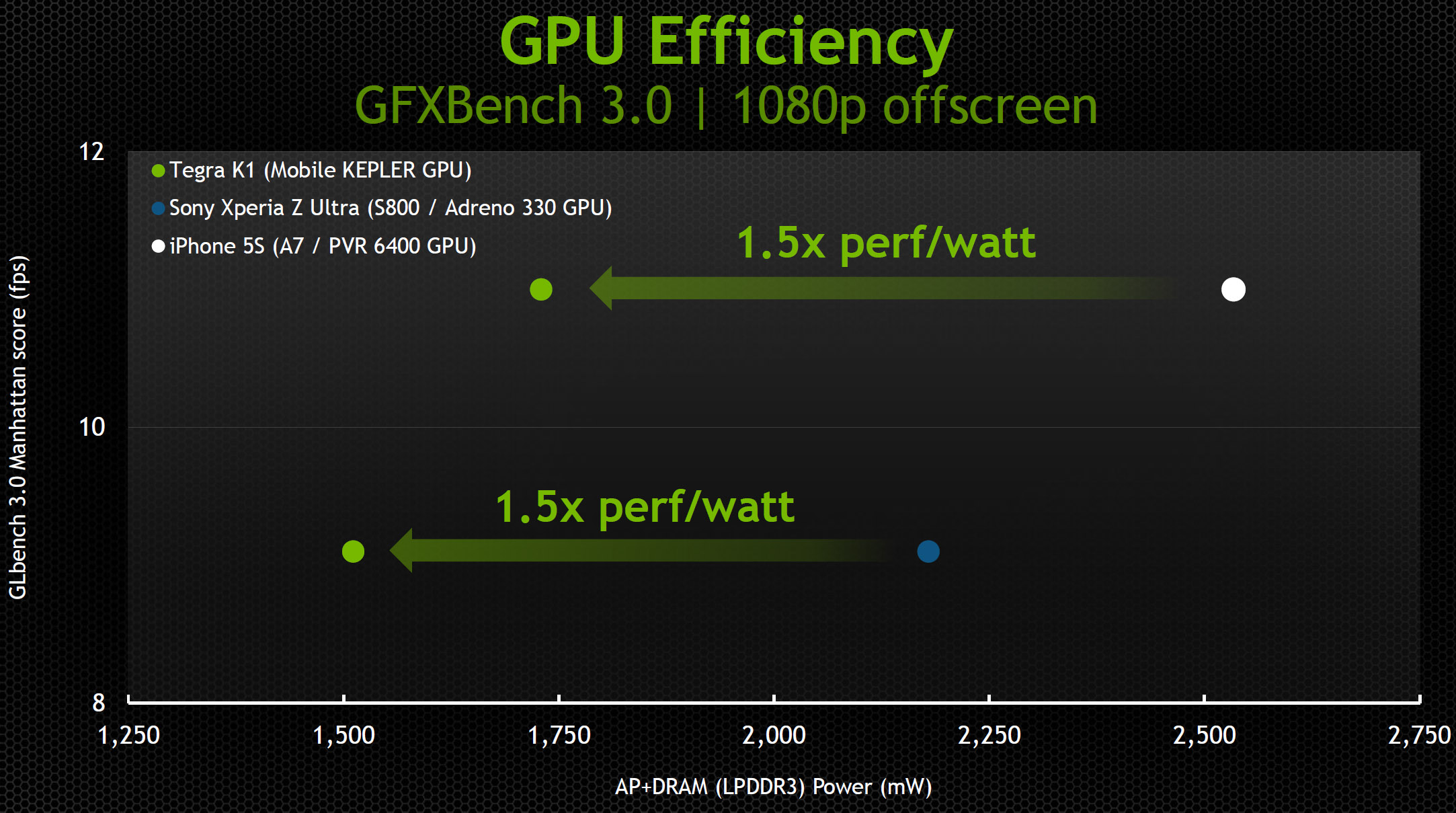
Nvidia presented its own benchmark results from the upcoming GFXBench 3.0, graphing framerate against power consumption in the 1080p Manhattan off-screen test. It chose Apple’s iPhone 5s and Sony’s Xperia Z Ultra as comparison points, targeting the A7 and Snapdragon 800 SoCs. At a constant performance level, the company claims a 1.5x performance per watt advantage over both with the application processor and DRAM power summed.
Current page: Tegra K1’s GPU: More Or Less One SMX
Prev Page Putting Kepler Into Tegra: It’s All About Graphics Next Page Chimera 2: Putting An Emphasis On Imaging-
RupertJr "Approx. Comparison To Both Last-Gen Consoles"Reply
Why don't you update the graph title to "Prev Gen Consoles" since last gen consoles has 1.23 TFLOPS (XBOX One) and 1.84 TFLOPS (PS4) performance difference to this K1 chip is huge. It looks like NVidia will loose another battle... -
renz496 Reply12372657 said:Where is the maxwell stuff did they not even address it yesterday? WTF
most likely they will talk about it when the actual gpu is close to release. -
Wisecracker ReplyAt least in theory, Tegra K1 could be on par with those previous-generation systems ...
AMD does it. Intel, too. But ...
When it comes to over-the-top hype, embellishment and hyperbole, nVidia is the king.
-
ZolaIII @ Rupert JrReply
Well multiplied 3x & with higher memory bandwidth you are there.
1.5x Maxwell & 2x cores (28nm to 16-14nm).
Hyper memory cube.
All this in 2015. -
RupertJr @ZolaIIIReply
but what you are assuming does not exists nowadays and maybe until years...
where will be other chips at that time? -
dragonsqrrl "in fact, the first Maxwell-powered discrete GPUs are expected in the next few weeks"Reply
Excellent. -
InvalidError Reply
Well, they are right on at least one thing: 2014's SoCs are now about on par with high-end components from ~7 years ago or mid-range gaming PCs from ~5 years ago and are managing to do so on a 2-3W power budget, which is rightfully impressive IMO.12373063 said:It looks like NVidia will loose another battle...
If SoCs continue improving at this pace while PCs remain mostly stagnant, the performance gap between SoCs and mainstream PCs will be mostly gone by the time 2015 is over. -
Shankovich I'm assuming this SoC will run at around 15 watts. With 192 CUDA cores and DDR3 LP, your max output will probably be somewhere around 180 GFLOPS. Yes yes it CAN do the same effects as consoles and PC, so what? If the Game Cube had DX 11.2 api running on it, it could as well, but obviouslt it coiuldn't put too much on the screen. This will be the same deal with the K1.Reply
It's cool, I like it, don't get me wrong, but the stuff they're saying, though technically correct, is so misleading to about 90% of the market. People are going to think they have PS4's in their hand when in reality they have half a xbox 360 with up to date API's running on it.


