AMD GPUs In 2016: Polaris Lights Up The Roadmap
When AMD introduced its GCN architecture late in 2011, the Radeon HD 7970 was doing battle against Nvidia’s Fermi-based GeForce GTX 580. Since then, the competition rolled out Kepler and Maxwell, improving performance-per-watt dramatically compared to its previous designs.
And yet, AMD continues to hold its own in terms of absolute performance. The Radeon R9 Fury X even bests its nemesis, the GeForce GTX 980 Ti, in most benchmarks at 3840x2160. But after launching the Radeon R9 380X back in November using another re-branded GPU, AMD knows it needs something more than aging technology at bargain-bin prices to revitalize its portfolio.
Polaris is the architecture it hopes will do that (and by "architecture," the company is no longer referring exclusively to graphics IP, but rather the whole SoC and its subsystems).
With availability planned for mid-2016, Polaris’ arrival could not come any faster. The Rift is expected to ship in Q1 2016, and Oculus’ hardware recommendations for a full VR experience start at a Radeon R9 290, leaving just a handful of cards from AMD and Nvidia capable of passing muster. Any graphics processor pushing higher frame rates or similar performance for less money is going to attract attention. An enthusiast-oriented version of Polaris should do both, while simultaneously improving AMD’s performance per watt in a major way.
We recently covered AMD’s plans to enhance Polaris’ display engine, including the addition of HDMI 2.0a and DisplayPort 1.3 support, along with the foundational work for HDR gaming, photos and movie playback. A follow-up described the company’s strategy to facilitate broader access to open source tools, effects and libraries through a new GPUOpen portal, plus a renewed effort in the HPC space with its Boltzmann initiative.
A High-Level Look Inside Polaris
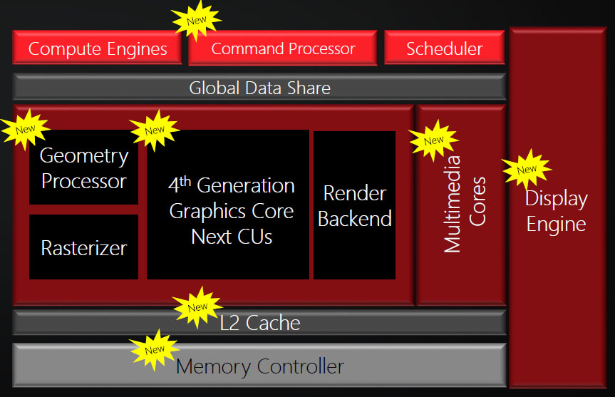
Today we get a slightly closer look at the hardware itself. Most telling, perhaps, is that Polaris includes fourth-generation Graphics Core Next IP, which may come to be known as "GCN 1.3" outside of AMD's walls.
That might disappoint enthusiasts who were hoping for a reimagined approach to efficiency, given the competitive landscape. However, there are a number of design tweaks specifically aimed at improving AMD’s standing in performance-per-watt. The company isn’t dishing on low-level details yet, but it does identify its new primitive discard accelerator, tuned hardware scheduler, better instruction pre-fetch capabilities, improved shader efficiency and memory compression as areas in the architecture that were reworked. Cumulatively, they, along with a major manufacturing milestone we’ll discuss shortly, facilitate what SVP and chief architect Raja Koduri claims to be the largest performance-per-watt jump in the company’s history (including ATI).
Get Tom's Hardware's best news and in-depth reviews, straight to your inbox.
AMD also isn’t saying much about the multimedia block mentioned on the right side of this slide, but it did acknowledge that Polaris will include hardware-accelerated H.265 decode at up to 4K with Main 10 profile support. That last bit means the GPU’s decoder supports 8- and 10-bits per sample, which turns into a critical puzzle piece in enabling the Rec. 2020 color space. As far as we can tell currently, Polaris doesn’t incorporate version two or three of the H.265 standard, which were approved in 2014 and 2015, respectively. H.265 encode should be possible at up to 4K60p, though we don’t know how much of that is handled by the shaders or implemented in fixed-function logic.
FinFET: Cramming More Into Less
Although AMD’s architects no doubt played a hand in the efficiency gains being attributed to Polaris, we might guess that transitioning from TSMC’s 28nm high-performance node to 14nm (GlobalFoundries)/16nm (TSMC) FinFET transistors yields even larger returns.
The idea of non-planar transistors isn’t new to Tom’s Hardware readers—we first met Intel’s closely-related tri-gate transistors in 2012, which served as the building blocks of its 22nm Ivy Bridge architecture. At the time, we knew competing foundries would be years behind with their equivalent processes, though not even AMD expected to pause for so long at 28nm. But now the company is getting the technology’s benefits—faster, lower-leakage transistors of a uniform structure, which are consequently subject to less variation.
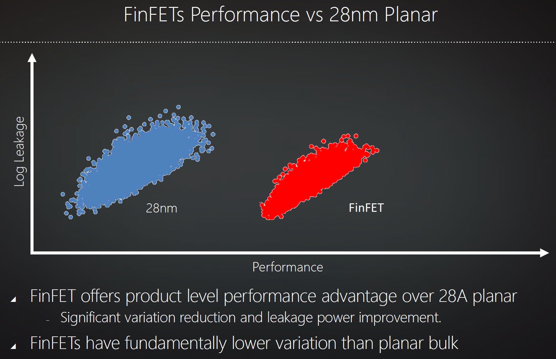
AMD’s Joe Macri illustrated the real-world advantages of FinFET compared to the 28nm planar node using the chart above. The non-linear y-axis represents leakage current with transistor performance plotted on the x-axis. Within each of those two “clouds” you have the available transistor characteristics, from lower-leakage, lower-performance (bottom-left) to higher-leakage, high-performance (top-right). Given FinFET’s position to the right of 28nm, you can conclude that, for any amount of leakage, you get more performance. In fact, Macri specifies a 20-35 percent performance advantage over 28nm.
Now, notice that the clouds aren’t the same size. FinFET’s narrower oval is indicative of less variation. That behavior is inherent to the way fins are etched. Instead of using transistors of different widths, which is problematic when “width” corresponds to fin height, they’re all created similarly and put together in parallel. What results is more consistent binning.
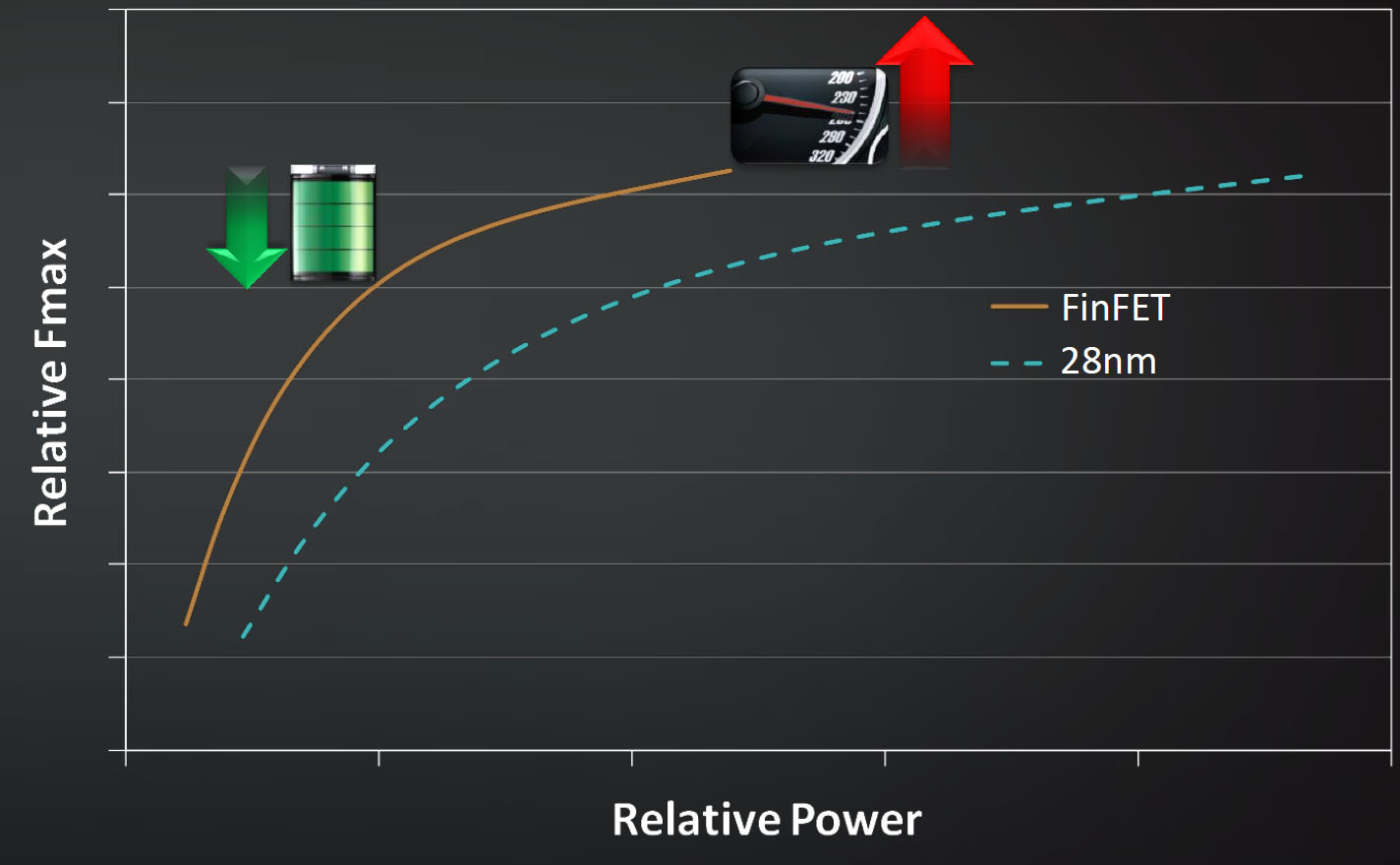
For a given product, comparing 14/16nm FinFET to 28nm planar yields these two performance over power curves. They represent new opportunities for AMD—more powerful desktop GPUs at today’s power targets, existing performance levels in smaller form factors, thin-and-light notebooks with discrete graphics, and so on. Of course, Nvidia has access to the same process technology, so it remains to be seen who has the advantage six months from now.
Polaris Is Already Up And Running
Even though we’re half a year away from expected availability, AMD had one surprise for the attendees of its RTG summit in Sonoma, CA that might suggest a timing advantage over its competition: the first Polaris-based GPU running Star Wars Battlefront after less than two months back from the fab. This isn’t going to be a desktop bruiser. Rather, AMD is looking to arm compact notebooks with a GPU capable of 1920x1080 at 60 FPS—a previously-unattainable milestone in the form factors it’s talking about.
So, in the demo we saw, AMD standardized on that 60 FPS performance mark and compared the power consumption of two Core i7-4790K-based platforms—one with Polaris and another with Nvidia’s desktop GeForce GTX 950—using the Medium quality preset. The system with AMD’s board averaged 86 W, whereas the other machine was closer to 140 W. Nvidia’s GTX 950 is a 90 W board, and we’ve seen it close to that figure. So, if you take 90 away from 140, you get about 50 W of system power use.
Although it didn’t do any additional math in its slides, AMD might have us believe that this implementation of Polaris is in the 36 W range. If true, that would put it in the ballpark of a GeForce 940M, based on GM108 with 384 shaders, at GeForce GTX 950’s performance. And AMD’s Koduri said his team is just getting started on optimizations for the GPU—about a dozen SoC-level power features haven’t been enabled yet.
We were left to wonder about shader count, clock rates and on-board memory, but we did discover that AMD is still using GDDR5 for this particular chip’s target market, and that the GPU itself was manufactured on GlobalFoundries’ 14nm process.
From Afar, Polaris Appears Bright
We’re cautiously optimistic. A mobile-first approach makes sense for AMD, given the potential to reclaim lost market share with compelling hardware and an early disclosure. And while the company chose to demo a processor designed for thin-and-light form factors, hoping to catch its OEM customers’ eyes early in their design cycles, representatives admit that AMD will also have a “larger” version ready close to the first GPU’s launch, presumably for the enthusiast crowd. Koduri deflected specific questions about HBM and Polaris, but he affirmed his commitment to the technology’s progression and mentioned sharing roadmap details in the near future
That’s a fairly long way off, and Nvidia is undoubtedly working on its own FinFET-plus-architecture message, as well. It remains to be seen whether a tuned version of GCN can hold off the competition in absolute performance and performance-per-watt, but it appears certain that AMD’s next-generation GPU lineup will offer a sizable step forward relative to the existing portfolio.
-
jimmysmitty Chris, another site claimed it was 16nm FinFETs not 14nm. I would assume your source is correct but is it 14nm for sure?Reply
And while I find this interesting and hopefully good for the GPU market I am not interested in the normal marketing. Can;t wait till you get your hands on one of these and Pascal to do a true equal review instead of some marketing slide mumbo jumbo. -
CelicaGT Reply17255054 said:Chris, another site claimed it was 16nm FinFETs not 14nm. I would assume your source is correct but is it 14nm for sure?
And while I find this interesting and hopefully good for the GPU market I am not interested in the normal marketing. Can;t wait till you get your hands on one of these and Pascal to do a true equal review instead of some marketing slide mumbo jumbo.
They are dual sourcing TSMC and Global Foundry. -
jimmysmitty Reply17255109 said:17255054 said:Chris, another site claimed it was 16nm FinFETs not 14nm. I would assume your source is correct but is it 14nm for sure?
And while I find this interesting and hopefully good for the GPU market I am not interested in the normal marketing. Can;t wait till you get your hands on one of these and Pascal to do a true equal review instead of some marketing slide mumbo jumbo.
They are dual sourcing TSMC and Global Foundry.
I know about the dual sourcing. That doesn't answer my question because dual sourcing could mean high end is 14nm, low end is 16nm or it could even mean a Apple 6S debacle where it is luck of the draw which one you get.
My question is to which is it and if there is a definitive source as to how it will work. -
chronium Reply17255109 said:17255054 said:Chris, another site claimed it was 16nm FinFETs not 14nm. I would assume your source is correct but is it 14nm for sure?
And while I find this interesting and hopefully good for the GPU market I am not interested in the normal marketing. Can;t wait till you get your hands on one of these and Pascal to do a true equal review instead of some marketing slide mumbo jumbo.
They are dual sourcing TSMC and Global Foundry.
I know about the dual sourcing. That doesn't answer my question because dual sourcing could mean high end is 14nm, low end is 16nm or it could even mean a Apple 6S debacle where it is luck of the draw which one you get.
My question is to which is it and if there is a definitive source as to how it will work.
You're not going to know until they announce the cards, they only announced the road map not the specifics. -
darcotech Hi,Reply
This looks to me like a right GPU for next Macbook pro 15 with Skylake CPU. can't wait. -
wifiwolf from other news you can see that tsmc only has 16nm and glofo only has 14nm. You have your answer.Reply -
Achoo22 Replynot ashamed to admit I only understood about 10% of this article. XD
That's because it uses a lot of words to say very little. The summary is that AMD hasn't released meaningful details on their upcoming products beyond that: they should arrive in six-ish months, they enjoy a process shrink that can't fail to increase efficiency, they will support 4k and h.265 at least partly in hardware. -
NightAntilli What's with the calling of everything AMD does 'rebrands'? If GCN 1.0 to GCN 1.1, and GCN 1.1 to GCN 1.2 is all rebrand, Maxwell to Maxwell 2 is also a rebrand.Reply -
voodoochicken Coupled with other technologies, this could be a boon for AMD in the mobile space. However, Intel might be providing more competition in this space than nVidia. Even IBM is a wildcard as far as feasibility in this segment.Reply


