Evolution Of Intel Graphics: i740 To Iris Pro
First-Generation Intel HD Graphics (2010)
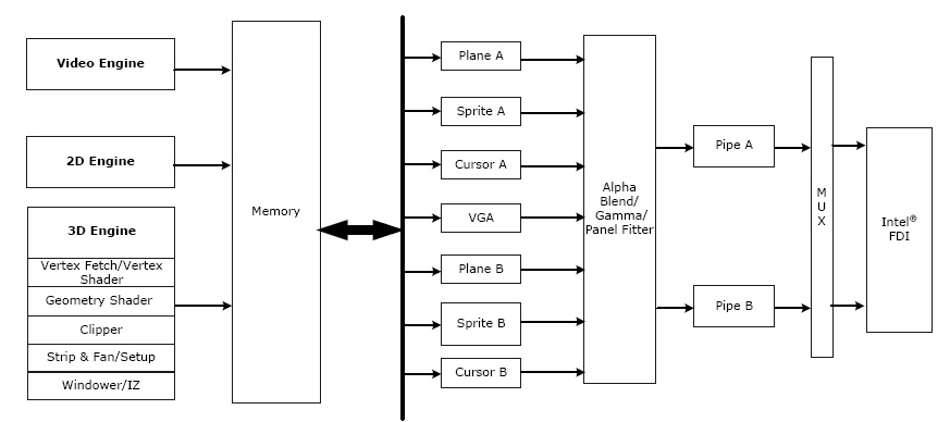
Intel introduced the HD Graphics product line in 2010 to pick up where the GMA family left off. The HD Graphics engine in the first-gen Core i3, i5 and i7 processors was similar to GMA 4500, except it had two additional EUs. Clock speed stayed about the same, ranging between 166MHz in low-power mobile systems and 900MHz on higher-end desktop SKUs. Although the 32nm CPU die and 45nm GMCH weren't fully integrated into a single piece of silicon, both components were placed onto the CPU package. This had the effect of reducing latency between the memory controller inside of the GMCH and the CPU. API support didn't significantly change between the GMA and HD Graphics implementations, though overall performance increased by over 50 percent.
Sandy Bridge: 2nd-Gen Intel HD Graphics (2011)
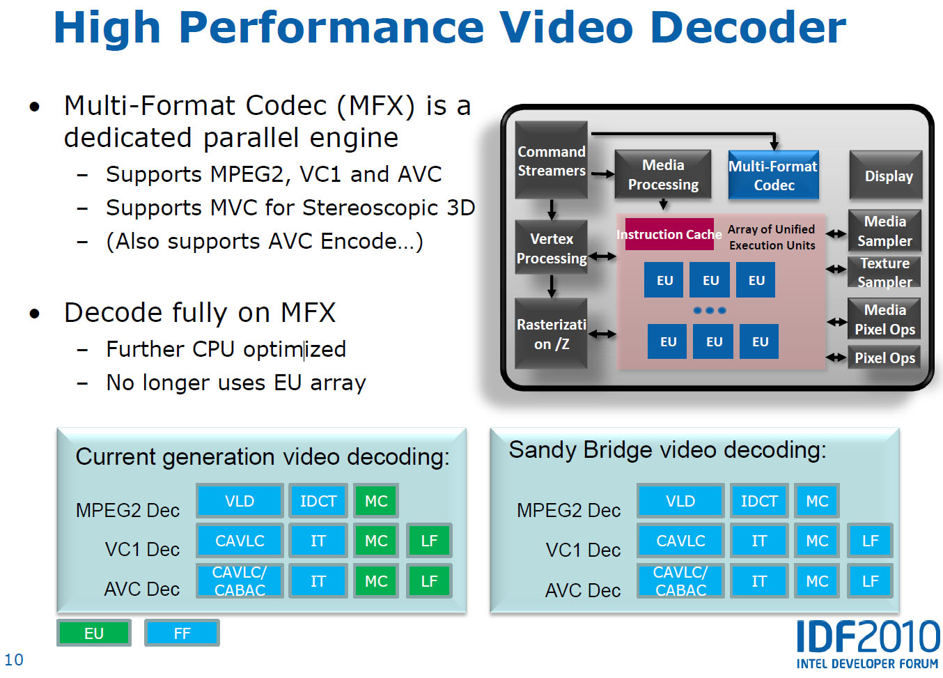
With Sandy Bridge, the Intel HD Graphics took another step up in terms of performance. Instead of placing two separate dies on one package, Intel instead merged the hardware into a single die, further reducing latency between the components. Intel also extended the graphics chip's feature set with Quick Sync technology for transcoding acceleration and a more efficient video decoder. API support didn't improve much, extending only to DirectX 10.1 and OpenGL 3.1, but clock speed increased significantly, ranging between 350 and 1350MHz.
With the wide range of features in play, Intel took the opportunity to segment its line-up. Low-end chips received HD branding (based on GT1 with six EUs and limited video decoding), mid-range solutions were HD 2000 (employing the same GT1 with six EUs, but full decode/encode hardware) and high-end SKUs received HD 3000 (GT2 with 12 EUs, plus the full benefits of Quick Sync.
Xeon Phi (2012)
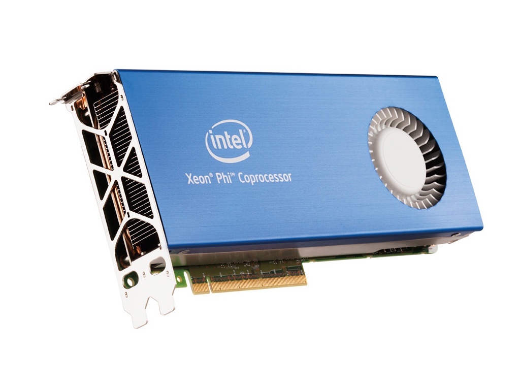
After Larrabee was cancelled, Intel shifted its design goals for the underlying technology. While Larrabee could have been quite capable for gaming, the company saw a future for it in compute-heavy applications and created the Xeon Phi in 2012. One of the first models, the Xeon Phi 5110P, contained 60 x86 processors with large 512-bit vector units clocked at 1GHz. At that speed, they were capable of more than 1 TFLOPS of compute horsepower, while consuming an average of 225W.
As a result of the high compute performance relative to power consumption, the Xeon Phi 31S1P was used in the construction of the Tianhe-2 supercomputer in 2013, which persists as the world's faster computer today.
Ivy Bridge: The Intel HD 4000 (2012)
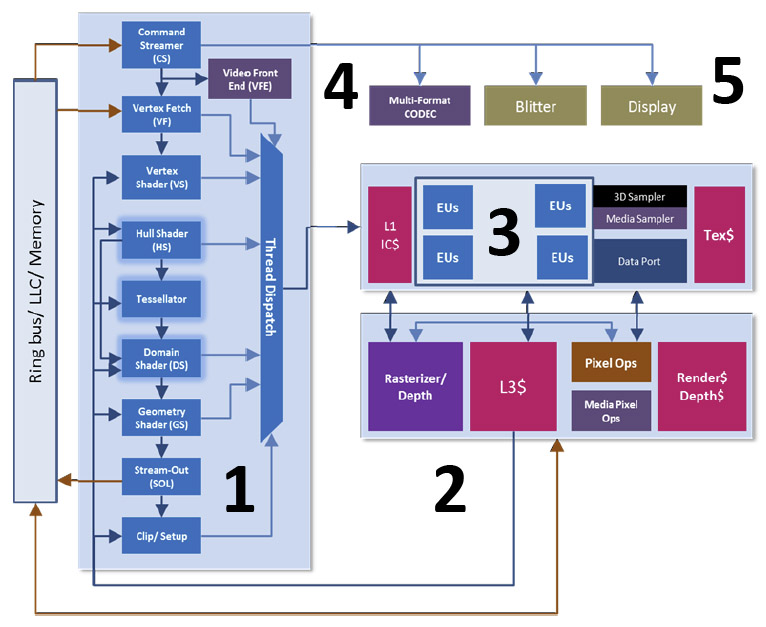
With the introduction of Ivy Bridge, Intel redesigned its graphics architecture. Similar to the Sandy Bridge iGPUs, Ivy Bridge was sold in three different models: HD (GT1 with six EUs and limited decoding/encoding), HD 2500 (GT1 with six EUs and complete decoding/encoding functionality) and the HD 4000 (GT2 with 16 EUs and complete decoding/encoding functionality). Operating at lower 1150MHz clock rates than the Intel HD 3000, but with four additional EUs, the HD 4000 was significantly faster, averaging a 33.9 percent performance increase in games like Skyrim. Part of this gain was attributable to an improved architecture, which moved to Pixel Shader 5.0, enabling DirectX 11.0 and OpenCL 1.2 support for the first time.
The performance of Intel's Quick Sync technology also increased significantly, capable of transcoding H.264 video files from one format to another over twice as fast. Hardware acceleration of video content was extended too, and the Intel HD 4000 was technically capable of decoding multiple simultaneous 4K steams.
Get Tom's Hardware's best news and in-depth reviews, straight to your inbox.
Intel Expands It's Graphics Line With Haswell (2013)
Architecturally, the HD Graphics engines released alongside Haswell are similar to those inside of Ivy Bridge, and can be viewed as an extension of the Ivy Bridge graphics core. Intel relied on sheer force in order to drive up GPU performance in Haswell. This time around, the company did away with the small six-6 EU model, opting to place 10 EUs inside of Haswell's GT1 implementation. Full video decoding was enabled, while other features like accelerated encoding and Quick Sync were turned off. Intel also further diversified its GPU offerings. The GT2 version, which contained 20 EUs, was used inside of three different graphics cores: HD Graphics 4200, 4400 and 4600. These models are mostly differentiated by clock rate.
Intel also introduced a higher-end model called GT3. It contained 40 EUs and was capable of significantly higher performance. CPUs with GT3 built-in were marketed under the HD Graphics 5000 and 5100 model numbers. The rare GT3e Intel Iris Pro 5200 variant included 128MB eDRAM on the CPU package, and was the first incarnation of Intel's Iris Pro family. Although the Iris Pro 5200 performed much better than the models without dedicated eDRAM, its impact on the market was limited since it appeared in so few high-end processors.
A low-power version of the Haswell iGPU with only four EUs was also used inside of the Intel Atom CPU, code-named Bay Trail. With the addition of the high-performance GT3 and the low-power Bay Trail variant, the Haswell iGPU included eight different products compared to only three in Sandy Bridge and Ivy Bridge.
Broadwell (2014)
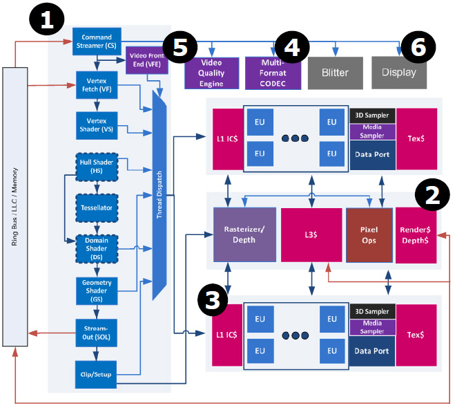
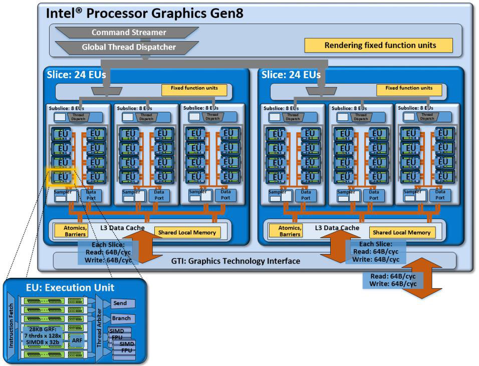
With Broadwell, Intel once again redesigned its iGPU so that it could scale more effectively. The architecture organized its EUs into sub-slices of eight. This made the process of adding EUs even easier as Intel could duplicate the subslice multiple times. The GT1 implementation contained two slices (although only 12 EUs are active). The next three products, HD Graphics 5300, 5500, 5600 and P5700, use the GT2 chip with 24 EUs (although some implementations only have 23 active EUs).
The high-performance GT3 and GT3e chips contain 48 EUs and are used in the HD Graphics 6000, Iris Graphics 6100, Iris Pro Graphics 6200 and Iris Pro Graphics P6300 models. Similar to the Haswell Iris Graphics products, the Broadwell Iris Graphics SKUs use the GT3e chip and include 128MB of integrated eDRAM memory. Each group of eight processing units shares 64KB of cache. These GPUs support DirectX 12, OpenGL 4.4 and OpenCL 2.0.
Skylake (2015)
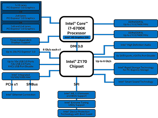
The latest version of Intel's graphics technology is used inside of the Skylake-based CPUs. These graphics chips are closely related to the Broadwell iGPUs, share the same architectural layout and keep the number of EUs essentially the same across the board. The biggest change with this generation is a change in the naming convention. Intel changed the nomenclature to the HD Graphics 500 series instead. The low-end HD Graphics and HD Graphics 510 models use the GT1 die with 12 EUs. The HD Graphics 515, 520, 530 and P530 use the GT2 chip with 24 EUs.
Starting with Skylake, Intel further divided the Iris and Iris Pro series of products. The Iris 540 and 550 will come with 48 EUs containing the GT3e graphics chip. It isn't clear what the core name will be for the Iris Pro 580, but it will contain a total of 72 EUs, and will likely be significantly faster than the Iris Pro 6200 graphics chip used inside of Broadwell. It isn't clear how much eDRAM these chips will have, but Intel will likely use this to further divide the performance of the Iris and Iris Pro graphics chips. The Iris 540 will have only 64MB of eDRAM, half that of the Broadwell GT3e. Intel hasn't stated the exact specs for the Iris Pro or Iris 550 graphics chip at this time, however.
Kaby Lake (2017)
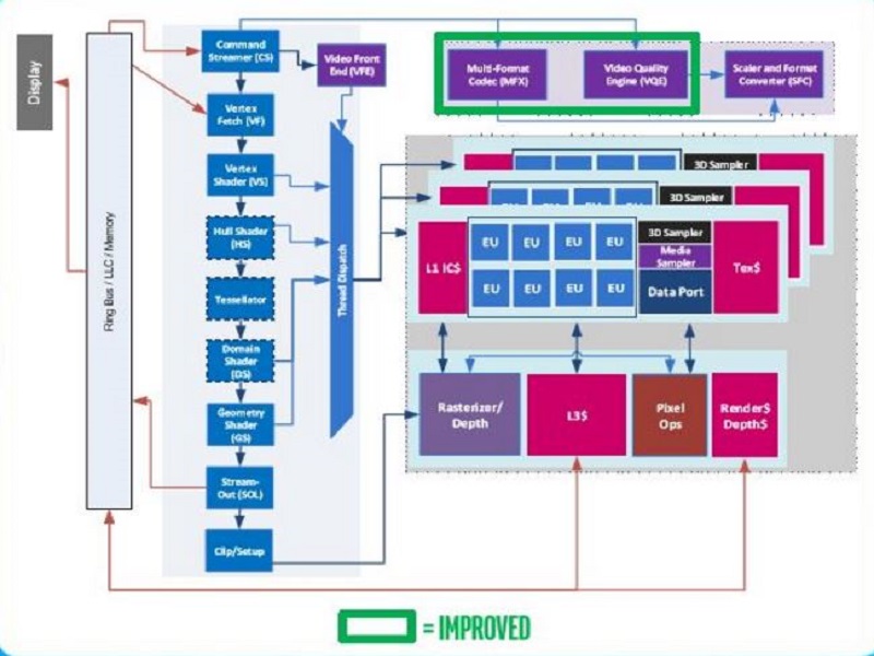
With the release of Intel’s Kaby Lake processors, Intel pushed out an improved iGPU: Intel HD Graphics 630. Like its predecessor, the HD 630 has 24 EUs and operates at similar clock speeds. Intel improved the fixed-function hardware used for decoding and encoding to support improved 4K playback and streaming. This also improved energy efficiency. Beyond that, the Intel HD Graphics 630 iGPU is essentially the same as the Intel HD Graphics 530 found inside of Skylake CPUs.
MORE: Best CPUs
MORE: Intel & AMD Processor Hierarchy
MORE: All CPU Content
-
adamovera Archived comments are found here: http://www.tomshardware.com/forum/id-2839510/evolution-intel-graphics-i740-iris-pro.htmlReply -
LucaFire Great read :) Been waiting for something like this; no one really covers the history of Intel's graphics/integrated solutions.Reply -
bit_user ReplyLarrabee (2009)
No, it was theoretically specified at 2 TFLOPS, while Nvidia's GTX 285 could manage 708 GFLOPS. That's still impressive, but not > 10x.
Picture 11 of 20
...
This FPU was theoretically specified at over 10 times more throughput than comparable Nvidia GPUs from the same time period.
Real world performance of Larrabee was demonstrated at ~1 TFLOPS.
Sources:
■ https://en.wikipedia.org/wiki/Larrabee_(microarchitecture)■ https://en.wikipedia.org/wiki/List_of_Nvidia_graphics_processing_units#GeForce_200_series
Xeon Phi (2012)
Perhaps you meant to say "one of the world's faster computers, today"? According to top500.org, Sunway TaihuLight is #1, displacing Tianhe-2 (MilkyWay-2) to #2.
Picture 14 of 20
As a result of the high compute performance relative to power consumption, the Xeon Phi 31S1P was used in the construction of the Tianhe-2 supercomputer in 2013, which persists as the world's faster computer today.
Oh, and it's really not a GPU, though I guess it's fair to include, here. Without Xeon Phi, Larrabee ends up looking like a complete dead end. Plus, the whole HD graphics story is pretty uninteresting, with no huge changes from one generation to the next (aside from the addition of optional eDRAM).
BTW, you could've added the Knights Landing generation (https://en.wikipedia.org/wiki/Xeon_Phi#Knights_Landing), again showing the progression of the architecture started by Larrabee. With OmniPath, HMC, and motherboard socket compatibility, this made Xeon Phi start to look very interesting. -
bit_user Reply
Sorry, the only mainstream console to use ARM processors, so far, is Nintendo Switch. XBox 360, PS3, and the last 3 non-portable Nintendo's used variants of PowerPC, while XBox One and PS4 are using AMD (x86-64) APUs.19277885 said:The consoles run big GPU's along side ARM processors...
Though, it's definitely true that the bulk of consoles' compute power is contained in the GPU. Same is true for many phones, tablets, and even Intel's desktop CPUs.
Speaking of consoles, I've always wondered if the original Haswell-era GT3e was originally developed as a bid to win the XBox One design. Microsoft has always had a thing for a chunk of fast, on-chip memory. XBox 360 and XBox One both have it, while neither PS3 nor PS4 went that direction.
This is actually pretty close to what the Xeon Phi is. The latest generation (codename: Knights Landing) is sort of a hybrid between a CPU and GPU, where they took low-power general-purpose CPU cores from their Atom product line and made them much more GPU-like.19277885 said:The fastest computer's will be an array of co-processors including GPU's
Check out their Tesla products: https://en.wikipedia.org/wiki/List_of_Nvidia_graphics_processing_units#Tesla19277885 said:Nvidia has not had to whip out it's ... and show it off yet.
As you can see from that table, they've been going after server & cloud computing for about 10 years, now. Intel is trying to keep up, but you're also correct that Nvidia holds a substantial lead in both raw compute and energy-efficiency.
http://www.nvidia.com/object/tesla-supercomputing-solutions.html -
bit_user Reply
I'm not sure about AMD's older APU offerings, but Ryzen-based APUs will definitely stomp all over them, in this area.19378146 said:Think about it, Intel's GPU are actually the best for what it is intended for
