


Two Times The Compute Power
Although AMD took the hardware community by surprise with the performance of RV770 and the derivative Radeon HD 4850/4870, things didn’t go entirely according to plan. The company launched its boards immediately after Nvidia, which turned around and slashed the prices on its own models, determined to win this round of the ongoing graphics card war.
And yet, a month and a half after the launch of AMD’s newest round of products, the verdict hasn’t changed. Neither the GeForce GTX 260 nor the GeForce 9800 GTX+ (only recently made available) can take on the Radeon HD 4870 with regards to price or performance, even in light of heavy cuts from Nvidia.

But AMD’s not out just to make waves with the gamers looking for value. It also wants to reclaim a crown it lost a long time ago to Nvidia’s last two generations of large, monolithic programmable graphics architectures. As a means to that end, the company is putting a pair of its most impressive GPUs on a single PCB and calling it the Radeon HD 4870 X2. Now the question remains: does the new board have the muscle to take on Nvidia’s GeForce GTX 280, the single fastest card?
The Radeon HD 4870 X2
Contrary to what its code name might otherwise suggest, the R700 actually centers on a design sporting two RV770 GPUs. Thus, the Radeon HD 4870 X2 finds itself in a very high-end segment of the discrete graphics market. However, in the next few weeks you will also be able to find a Radeon HD 4850 X2, based on the same two chips but with lower frequencies and likely less memory as well.

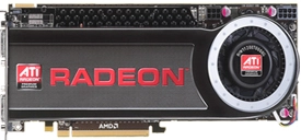
In appearance, the Radeon HD 4870 X2 remains similar to the Radeon HD 3870 X2. However, looks can be deceiving, as we will soon see. Not surprisingly, the card itself is quite long (26.7 cm). It sports a large blower that exhausts through the back of the board and is neighbored by two dual-link DVI outputs (neither HDMI nor DisplayPort connectivity are native to the back panel). The board requires two auxiliary power connectors—one with six pins and another with eight (PCI Express 2.0-compliant). The two GPUs are positioned on the same PCB, though you won’t see them since a heatsink/fan combination covers the entire board.
This card, like it’s bi-GPU flagship predecessor, must deal with sharing its frame buffer. But contrary to CPUs and their more complex memory management techniques, these things evolve a lot more slowly in the graphics card world. By comparison, all of the bi-GPU cards up until now were similar to the Pentium D 900 (Presler), acting as an assembly of two cores functioning independently and integrating their own local memory (L2 cache for the CPU, frame buffer for the GPU). All of the graphics data is thus duplicated between the two cards. Communication between them passes through an external bus—think FSB for Intel’s Pentium D and PCI Express for these graphics cards.

As with the Radeon HD 3870 X2, a PCI Express bridge manages the communications between the two GPUs and the chipset. Once the final display outputs is calculated, each GPU sends them to another chip that assembles the result according to whichever multi-card rending technology is used (AFR, most often) and then sends it all to the monitor. Back when we tested the Radeon HD 3870 X2, we found that the biggest impact on performance was attributable to the board’s memory capacity, since memory on a bi-GPU card has to be divided in two. And in order to assure adequate performance, you often have to multiply the quantity of memory by four, which is what AMD does with the 4870 X2.