AMD A8-3850 Review: Llano Rocks Entry-Level Desktops
Earlier this month we previewed AMD's Llano architecture in a notebook environment. Now we have the desktop version with a 100 W TDP. How much additional performance can the company procure with a loftier thermal ceiling and higher clocks?
A Word On Overclocking Llano
Llano goes heavy on integration. AMD purposely locked clock multipliers up and down the family. And yet the company suggests you can get 30%-better 3DMark Vantage scores by cranking the reference clock up to 133 MHz and dropping the multiplier (you can go down, but not up). Because the platform’s clock generator is integrated (like Intel’s P67/H67/Z68), though, messing with the reference frequency also overclocks the northbridge, graphics core, and PCI Express bus.
Well, the faster northbridge is fairly resilient, and you can use memory dividers to bring your RAM back down into spec. Moreover, the faster graphics core is actually a welcome speed-up—that’s how you’ll end up with better frame rates in games. But the overclocked PCIe bus can be a problem.
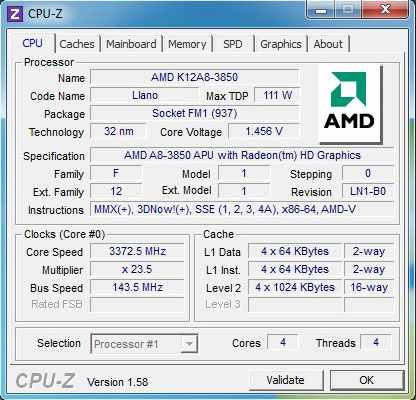
I spent a couple of late nights chatting back and forth with the fine folks at ASRock and Gigabyte, who helped in near real-time with BIOS builds. Eventually, I was able to get Gigabyte’s A75M-UD2H dialed in at nearly 3.4 GHz (it’d run in excess of that, but crashed under load) using a 23.5x multiplier and 145 MHz reference clock reflected as 143.5 MHz. The APU only needed a .05 V bump to achieve those numbers, too.
The problem was that I couldn’t use an SSD. Anywhere over a 110 MHz reference clock and the SSD simply ceased to be detected by the board’s BIOS. Even with a hard drive installed it’d sometimes take three or four reboots for the firmware to detect my disk. This is a known behavior Gigabyte is trying to mitigate, but it’s symptomatic of pushing clock rates system-wide beyond-spec. ASRock had a different issue with the elevated reference clock: losing USB 3.0 functionality. Other boards simply wouldn’t overclock well at all, failing long before we were forced to fight a bus speed idiosyncrasy.
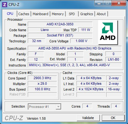
Pushing the A8-3850’s four cores from 2.9 GHz to 3.4 GHz is sure to benefit performance in processor-bound benchmarks, but it didn’t do nearly as much for gaming as simply installing faster memory.
At the end of the day, overclocking Llano is like slapping an intake on a Ford Fiesta. You’re not buying the thing for its potential on the track. You’re getting it because it’s inexpensive and “fast enough” to serve as a capable daily driver.
The idea of setting integrated graphics world records is humorous not because I’m a pretentious jerk, but because you could buy a Phenom II X3 720 Black Edition for $70 and a 1 GB Radeon HD 6570 for $70 and get better graphics performance right out of the box, in addition to an unlocked CPU sporting 6 MB of shared L3 cache. If you’re an overclocker, that could very well be the route to take. Llano is all about something else entirely.
Get Tom's Hardware's best news and in-depth reviews, straight to your inbox.
Is There A Future In Llano-Based Overclocking?
Several of the boards I tested had fields for higher multiplier settings and adjustable graphics clocks. Of course, turning those knobs doesn’t actually do anything on an APU with locked ratios. So why the heck are those settings exposed?
According to my sources, AMD plans to sell a Black Edition APU based on the Llano architecture. I don’t have a time frame. However, should we get access to unlocked CPU and GPU ratios, it’d become much easier to push each component of this 32 nm part as far as possible without running afoul of interfaces without as much tolerance for scaling.
Current page: A Word On Overclocking Llano
Prev Page Making Memory Performance Matter Again Next Page Test Setup And Benchmarks-
SteelCity1981 So then what's the point of getting the Turbo Core versions when they are going to be Turbo Clocked slower then the none Turbo Clocked versions...Reply -
cangelini SteelCity1981So then what's the point of getting the Turbo Core versions when they are going to be Turbo Clocked slower then the none Turbo Clocked versions...Reply
They don't want you to see better performance from a cheaper APU in single-threaded apps by pushing Turbo Core further ;-) -
Known2Bone i really wanted see some amazing gains in the content creation department what with all that gpu power on chip... oh well games are fun too!Reply -
ivan_chess I think this would be good for a young kid's PC. It would be enough to run educational software and a web browser. When he grows up to be a gamer it would be time to replace the whole machine anyway.Reply -
DjEaZy ... it's may be not the greatest APU for desktop... but it will be a powerful thingy in a laptop... the review was nice... but in the gaming department... would be nice to see a standard 15,x'' laptop resolution tests @ 1366x768... or something like that...Reply -
Mathos Actually if you want good DDR3 1600 with aggressive timings, the Ripjaws X series memory that I have does DDR3 1600 at 7-8-7-24 at 1.5v, not all that expensive when it comes down to it either.Reply -
Stardude82 This makes little sense. An Athlon II X3 445 ($75) and a HD 5570 ($60, on a good day you can get a 5670 for the same price) would provide better performance for the same price ($135) and not have to worry about the RAM you use.Reply
So is AM3+ going to be retired in favor of FM1 in the near future? Why are there chipset at all? Why isn't everything SOC by now?
Otherwise this is a very good CPU. If AMD has used 1 MB level 2 caches in their quads when they came out with the Deneb Propus die, they would be much more competitive. -
crisan_tiberiu stardude82This makes little sense. An Athlon II X3 445 ($75) and a HD 5570 ($60, on a good day you can get a 5670 for the same price) would provide better performance for the same price ($135) and not have to worry about the RAM you use. what about power consumption?Reply


