Ultimate X79? Five $320+ LGA 2011 Motherboards, Reviewed
Our flagship motherboard comparison announcement was answered with an interesting selection of models, along with a bunch of “not ready yet” responses. Today we examine a few samples from companies bold enough to step up to the plate during launch week.
X79 Overclocking
| BIOS Frequency and Voltage settings (for overclocking) | |||||
|---|---|---|---|---|---|
| Row 0 - Cell 0 | ASRock X79 Extreme9 | Asus P9X79 Deluxe | Asus P9X79 WS | Gigabyte G1.Assassin2 | Gigabyte X79-UD5 |
| Base Clock | 90-300 MHz (1 MHz) | 80-300 MHz (0.1 MHz) | 80-300 MHz (0.1 MHz) | 80-333 MHz (0.01 MHz) | 80-333 MHz (0.01 MHz) |
| CPU Multiplier | 12x to 60x (1x) | 12x to 57x (1x) | 12x to 57x (1x) | 12x to 59x (1x) | 12x to 59x (1x) |
| DRAM Data Rates | 800-2400 (266.6 MHz) | 800-2666 (266.6 MHz) | 800-2666 (266.6 MHz) | 800-3200 (266.6 MHz) | 800-3200 (266.6 MHz) |
| CPU Vcore | 0.60-1.52 V (5 mV) | 0.80-1.70 V (5 mV) | 0.80-1.70 V (5 mV) | 0.80-1.74 V (5mV) | 0.80-1.74 V (5mV) |
| VTT Voltage | 0.86-1.71 V (13 mV) | 1.05-1.70 V (6.25 mV) | 1.05-1.70 V (6.25 mV) | 0.72-1.61 V (5mV) | 0.72-1.61 V (5mV) |
| X79 PCH Voltage | 0.73-1.91 V (13 mV) | 1.10-1.70 V (6.25 mV) | 1.10-1.70 V (6.25 mV) | 0.87-1.98 V (5 mV) | 0.87-1.98 V (5 mV) |
| DRAM Voltage | 1.20-1.80 V (15 mV) | 1.20-1.99 V (5 mV) | 1.20-1.99 V (5 mV) | 0.83-1.51 V (5 mV) | 0.83-1.51 V (5 mV) |
| CAS Latency | 4-15 Cycles | 3-15 Cycles | 3-15 Cycles | 5-12 Cycles | 5-12 Cycles |
| tRCD | 4-15 Cycles | 4-15 Cycles | 4-15 Cycles | 5-31 Cycles | 5-31 Cycles |
| tRP | 4-15 Cycles | 4-15 Cycles | 4-15 Cycles | 5.15 Cycles | 5.15 Cycles |
| tRAS | 9-63 Cycles | 4-40 Cycles | 4-40 Cycles | 5-63 Cycles | 5-63 Cycles |
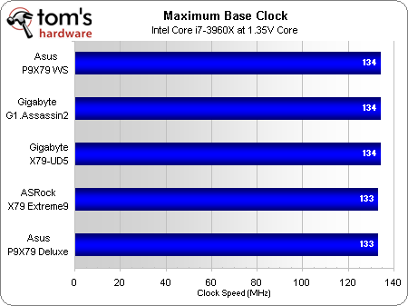
The addition of boot straps (chipset to CPU base clock ratios) to the LGA 2011 platform should have made overclocking easier compared to multiplier-locked LGA 1155-based CPUs, and yet every manufacturer appears to have figured out a way to make the process more difficult. ASRock, for example, make it clear where the ratios take effect as you scale up and down the base clock range. Altering Gigabyte’s base clock control by only 0.1 MHz caused boot failures with both motherboards when used in conjunction with higher-than-stock (33x) CPU ratios, leaving 100.00 and 125.00 MHz as our only overclocking options.
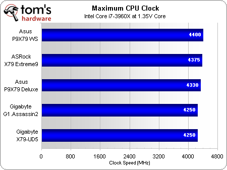
Asus’ limits were least-intrusive and appeared to be caused by changes in C1 core stepping power controls (a lower thermal throttling limit is one change that's easy to identify). We tried maxing out all of the settings we knew might help, but to no avail. Even still, 4.4 GHz at a mere 1.35 V core is nothing to be ashamed of.
We retested with a C0 Core i7 and shot straight to 4.7 GHz. We won't bother breaking down the settings we used to achieve that frequency because we don't want anyone to form expectations about a processor they can't actually buy. We'll instead keep testing whatever production-era samples we can get in hopes of finding a better example of Sandy Bridge-E's potential.
Once we figured out how ASRock's automatic adjustment worked, we were able to push our processor to a similar frequency as those achieved on both Asus boards. ASRock had also contacted us to say that it discovered the same C1-oriented multiplier problem in one of the 40 CPU samples it tested, credited a competitor with finding a workaround (we like that kind of honesty), and further stated that its team has developed a similar workaround we should have access to in mid-December. Since that's when the testing starts for our next round-up, we'll have a good opportunity to hold ASRock to that promise and report back to you.
Gigabyte’s results don’t look bad, but we were unable to overclock beyond stock Turbo Boost limits using multiplier adjustment alone. We were instead forced to use the 1.25x boot strap with a 34x multiplier and leave the 100 MHz base clock well enough alone.
Intel’s P67 X79 chipset still has the same 107-108 MHz limitation we've endured from mainstream Sandy Bridge platforms for the past 11 months. Boot straps multiply that range by 1.25x (and higher), though we were not able to reach the 166 or 250 MHz straps with our processor.
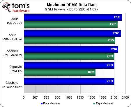
Asus has the best DRAM data rates, its P9X79 WS and P9X79 Deluxe taking first and second place.
Get Tom's Hardware's best news and in-depth reviews, straight to your inbox.
Current page: X79 Overclocking
Prev Page Power, Heat, And Efficiency Next Page Which High-End X79 Motherboard Is Best?-
lradunovic77 Something is wrong with your ASRock Extreme 9 testing. You article states that you used BIOS 1.40 however first release for this Motherboard was 1.60 and they also recently released 1.70. Bios 1.40 is for ASRock Extreme 4 which i own as well. Again in mean time they updated BIOS for ASRock Extreme 4 to version 1.50 which greatly improves overclocking. I have C1 and i am hitting 4.4Ghz easily. (1.50 BIOS ASRock Extreme 4).Reply
You might want re check the facts.
Thanks. -
Crashman lradunovic77Something is wrong ...You might want re check the facts.Please do verify the facts beginning with the first X79 Extreme9 UEFI screenshot on page 3, showing version P 1.40 . The latest public firmware was downloaded for every motherboard on November 18, which is before ASRock says its P1.60 was even published. And, if you check Newegg, you'll find that Newegg was actually selling the X79 Extreme9 before firmware P1.60 was published.Reply
How could that happen? ASRock has repeatedly removed previous BIOS versions from its website and labeled the replacement as the initial release.
This review was published after many hours of collaboration with ASRock, and some of the problems with this specific CPU are further detailed in the overclocking section. ASRock acknowledged the problem exists with a portion of the C1 CPU supply and has begun issuing patched BIOS to fix the multiplier issue, according to ASRock engineer William Yu. -
oxxfatelostxxo ReplyI have C1 and i am hitting 4.4Ghz easily. (1.50 BIOS ASRock Extreme 4).
Not to mention that they didnt say they couldnt hit 4.4ghz, they just stated they didnt get that high without going beyond 1.35v
Kinda wish we got to see a MAX overclock for air before temps got out of control =P
But then you get various coolers involved... yada yada... but PLEASE anyway -
clonazepam This was a fun article to read. I wanted to quote a few bits here and there just to point out I enjoyed the humor in it, but that would have been a lot of quotes. It's subtle, tasteful way to add personality to the piece.Reply
I had to comment on something. I can't really comment on the hardware as its so enthusiast and SB-E is well beyond my needs. I can't comment too much on the bios because I still barely understand mine, but I am seeing the trend that it might be best to stick with what you know, or risk having to translate the various names/definitions of settings across different products. I'm not that smart nor that patient. I liked the comment on the 6.00...lol... %! I never would have thought. I think that just deciphered half of my bios options, thanks. /wink -
In the comparison table on the ASUS : "6 (x16/x0/x4/x16/x4/x0 or x8/x8/x4/x8/x84/x8)" -- x84 seems somewhat unlikely ;-)Reply
-
gmcizzle Not surprised both Asus boards came out on top performance wise, on most of these mobo roundups they usually do.Reply -
Steveymoo Without trying to sound critical, wouldn't it be prudent to test SLI scaling on these enthusiast boards? 1, 2, and 3 way SLI, extra PCI-E bandwidth is one of the main reason why people even bother splashing out the extra cash on these chipsets. (Aside from the extra epeen++)Reply
Just sayin' -
Crashman shstoneIn the comparison table on the ASUS : "6 (x16/x0/x4/x16/x4/x0 or x8/x8/x4/x8/x84/x8)" -- x84 seems somewhat unlikely ;-)Thanks. Yes, the x4 stays the same. Fixed!SteveymooWithout trying to sound critical, wouldn't it be prudent to test SLI scaling on these enthusiast boards? 1, 2, and 3 way SLI, extra PCI-E bandwidth is one of the main reason why people even bother splashing out the extra cash on these chipsets. (Aside from the extra epeen++)Just sayin'You obviously don't understand the value of those +++'s!Reply -
AstroTC AsRock has the better looking MB by far...Reply
Question does tht little fan on the motherboard get loud? If it does that would be a deal breaker for me -
CaedenV the problem with testing mobos is that they all have the same core (in this case the x79) which is what determines the raw speed of the system and busses, so they are all pretty well bunched together with no possibility of seeing any real world difference between boards. The things that differentiate the boards is in their feature sets, and as they are all rather different there is no proper way to test them against one another. Add to that the fact that these are all brand new boards which will see improvements with new UEFI releases, and there is really no way to pick a clear winner.Reply
On a side note I would love to see how these boards look assembled :)


