RAM Wars: Return of the JEDEC
Get Tom's Hardware's best news and in-depth reviews, straight to your inbox.
You are now subscribed
Your newsletter sign-up was successful
Latency
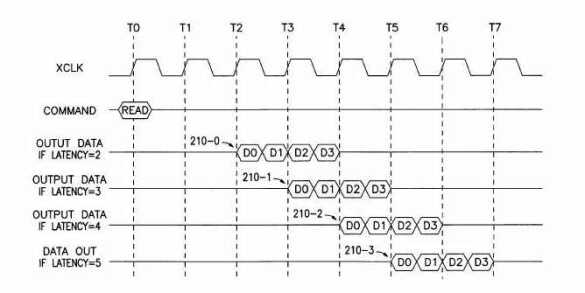
Based on Micron's patent for its multiple prefetch output data path technology, a timing diagram during a memory operation at five various latency settings is shown here.
A DRAM memory array can be thought of as a table of cells. These cells are comprised of capacitors, and contain one or more 'bits' of data, depending upon the chip configuration. This table is addressed via row and column decoders, which in turn receive their signals from the RAS (Row Address Strobe) and CAS (Column Address Strobe) clock generators. In order to minimize the package size, the row and column addresses are multiplexed into row and column address buffers. For example, if there are 11 address lines, there will be 11 row and 11 column address buffers. Access transistors called 'sense amps' are connected to each column and provide the read and restore operations of the chip. Since the cells are capacitors that discharge for each read operation, the sense amp must restore the data before the end of the access cycle.
The capacitors used for data cells tend to bleed off their charge, and therefore require a periodic refresh cycle or data will be lost. A refresh controller determines the time between refresh cycles, and a refresh counter ensures that the entire array (all rows) is refreshed. Of course, this means that some cycles are used for refresh operations, and this has some impact on performance.
A typical memory access would occur as follows. First, the row address bits are placed onto the address pins. After a period of time the RAS\ signal falls, which activates the sense amps and causes the row address to be latched into the row address buffer. When the RAS\ signal stabilizes, the selected row is transferred onto the sense amps. Next, the column address bits are set up, and then latched into the column address buffer when CAS\ falls, at which time the output buffer is also turned on. When CAS\ stabilizes, the selected sense amp feeds its data onto the output buffer.
Get Tom's Hardware's best news and in-depth reviews, straight to your inbox.
