Two Xeon CPUs Are Better Than One Intel P4 Extreme Platform
E7505/Placer Chipset Technology In Detail
The Intel E7505 chipset, code named "Placer," is based on a 180-nanometer process and is designed for two processors. The chipset has the same FC-BGA package as the 875/Canterwood, therefore it also has the same number of 1,005 soldering balls.
With 143 mm2, the surface size of the silicon die seems bigger, because the 875 requires only 100 mm2. The HUB 2.0 interface and the memory controller account for the larger surface area. This also keeps the price low for the motherboard manufacturers. For the E7505, you have to pay $100 per unit in quantities of 1,000 - twice as much compared to the 875.
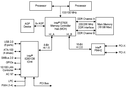
E7505 chipset as a block diagram
The E7505 Northbridge from Intel
The E7505 Northbridge (a.k.a. Memory Controller Hub, abbreviated as MCH) is typically bundled with the ICH4 and P64H2 Southbridge. The ICH4 is connected to the HUB 1.5 interface and clocks a speed of 66 MHz. This interface can transfer files to Northridge at a maximum speed of 266 MB per second with an 8 bit bus width.
Get Tom's Hardware's best news and in-depth reviews, straight to your inbox.
Current page: E7505/Placer Chipset Technology In Detail
Prev Page A Dual Vs. Single Processor Price Comparison Next Page E7505/Placer Chipset Technology In Detail, ContinuedTom's Hardware is the leading destination for hardcore computer enthusiasts. We cover everything from processors to 3D printers, single-board computers, SSDs and high-end gaming rigs, empowering readers to make the most of the tech they love, keep up on the latest developments and buy the right gear. Our staff has more than 100 years of combined experience covering news, solving tech problems and reviewing components and systems.