ASML delivers cutting-edge new chipmaking tool — third-generation EUV enables 2nm processors and beyond
Chipmakers need speed; ASML is here to deliver.

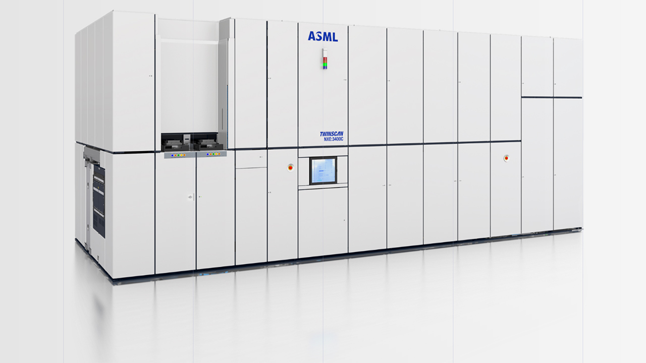
This week, ASML delivered its 3rd Generation extreme ultraviolet (EUV) lithography tool, the Twinscan NXE:3800E, with a projection lens featuring a 0.33 numerical aperture. The system significantly increases performance compared to the existing Twinscan NXE:3600D machine. It is designed for fabricating chips at leading-edge technologies, including 3nm, 2nm, and small nodes in the next few years.
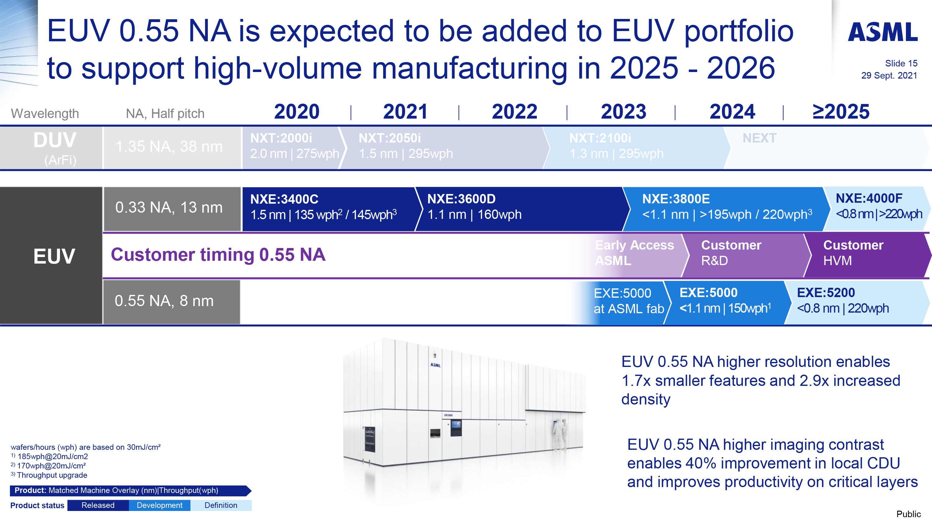
The ASML Twinscan NXE:3800E represents a leap forward in Low-NA EUV lithography regarding performance (the number of wafers processed per hour) and matched machined overlay. The new system can process over 195 wafers per hour at a 30 mJ/cm^2 dose and promises a further increase in performance to 220 wph with a throughput upgrade. In addition, the new tool offers a less than 1.1 nm-matched machine overlay (wafer alignment accuracy).
"Chipmakers have a need for speed," ASML revealed in a statement published on X. "The first Twinscan NXE:3800E is now being installed in a chip fab. With its new wafer stages, the system will deliver leading edge productivity for printing advanced chips. We are pushing lithography to new limits."
Increased throughput will increase the economic efficiency of the Twinscan NXE:3800E machine when producing chips on 4nm/5nm and 3nm-class process technologies for logic makers. The improved performance of ASML's Twinscan NXE:3800E is expected to significantly mitigate one of the primary drawbacks of EUV technology, which is its relatively low performance, thereby enabling more efficient and cost-effective chip production. This will make process technologies that rely on EUV more accessible to chip designers with budgets that are not as vast as those of Apple, AMD, Intel, Nvidia, and Qualcomm. Also, the tool will be crucial for memory makers such as Micron, Samsung, and SK Hynix.
In addition, the Twinscan NXE:3800E's enhanced performance will be particularly useful for making chips on 2nm and subsequent classes of fabrication technologies that will need EUV double patterning. Improvements in the matched machine overlay will benefit sub-3nm-class production nodes.
However, the sophistication and capabilities of machines like the NXE:3800E come at a substantial cost, with a price tag of around $180 million each. Such high costs mean it takes some time to depreciate the costs of these lithography tools. However, for ASML's clientele, which comprises a select group of significant logic and memory fabrication companies, the NXE:3800E offers a path to bolster their production capabilities of cutting-edge chips. This is crucial for these companies as they strive to meet the growing global demand for semiconductors, expand their production capacities, and manage the economics of chip manufacturing. Introducing more advanced and efficient EUV scanners like the NXE:3800E is critical to achieving these objectives.
Looking ahead, ASML is not resting on its laurels, with plans for further innovation in the form of the Twinscan NXE:4000F, another generation of Low-NA EUV scanner, slated for release around 2026. This ongoing development underscores ASML's commitment to advancing Low-NA EUV manufacturing technology despite the looming adoption of High-NA litho tools.
Get Tom's Hardware's best news and in-depth reviews, straight to your inbox.

Anton Shilov is a contributing writer at Tom’s Hardware. Over the past couple of decades, he has covered everything from CPUs and GPUs to supercomputers and from modern process technologies and latest fab tools to high-tech industry trends.
-
DavidLejdar Nice! I have no clue, which company will make the most use of it. But among ETF savings plan running, I have one for semiconductors in general, sort of providing capital for the investments needed. And once I have a bit on the side, as a rainy day fund to be able to buy e.g. a new pair of shoes or a fridge (in pension, or earlier if for some reason unemployed), in a about a year or two, I might upgrade my HW with something from the Twinscan NXE:3800E.Reply
Still waiting for some better innovations, which make use of improved technology though. Like, improved processors will likely show in improved versions of smartphones, tablets and laptops (and standalone AR/VR). But there is also the option to use e.g. a tablet to remote connect to own rig at home (over the internet). And in that context, it would be nice if there were some hand-held devices, which save a bit of money on the processing power, but have a top screen. That might not be a large market in regard to customers with a rig. But with improved internet connections, i.e. video game streaming may see some growth - and such a device could arguably help to keep the entry cost low (while also providing some workload for the upgraded data centers). -
P.Amini Reply
Good thing is TSMC is already using ASML as its tool and will buy this tool too!sjkpublic said:Ditto. Nice! Good thing they are not based in Taiwan. 2nm is the future.
