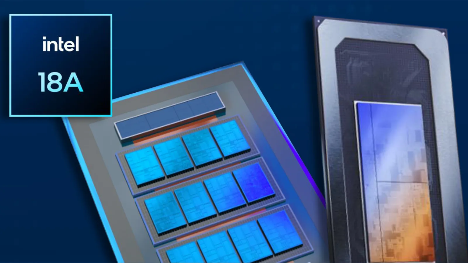
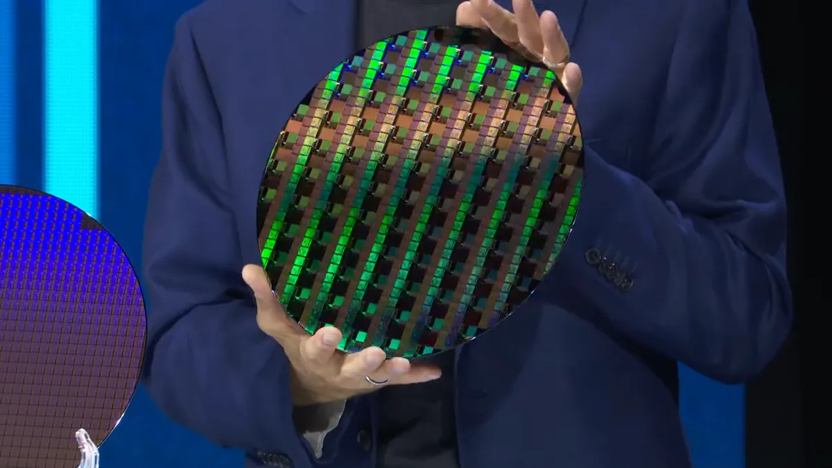
Nvidia and Broadcom are both testing chips using Intel's new 18A manufacturing process, reports sources to Reuters, indicating that these well-known projects continue. Intel's 18A process is the company's first fabrication technology to rely on gate-all-around RibbonFET transistors and a backside power delivery network named PowerVia. The Intel 18A process is broadly comparable to TSMC's N2 node. However, 18A is thought to be faster, while N2 is a denser chip.
Reuters sources suggest that both Nvidia and Broadcom's tests are not being conducted on complete chip designs, but the companies want to understand how 18A works in both behavior and performance. It's common to test processors before committing to purchasing them outright.
This isn't entirely new information, as there have been reports that Broadcom had been testing 18A since as early as September 2024. Back then, it was claimed that Broadcom's tests using 18A did not meet expectations, but that was not confirmed, with Broadcom merely saying the tests were ongoing.
Intel recently launched a dedicated website to advertise its 18A process, and consumer Panther Lake processors are set to enter mass production in mid-2025.
An Intel spokesperson told Reuters: "We don't comment on specific customers but continue to see strong interest and engagement on Intel 18A across our ecosystem."
(Image credit: Tom's Hardware)
While Intel's 18A process is reportedly garnering interest from big-name clients, Reuters claims to have reviewed supplier documents that indicate a problem with some unnamed third-party IP providers. Reuters claims this situation is causing "potential further delays in Intel's ability to deliver chips for some contract manufacturing customers" that could stretch the launch times for small and mid-size customers to mid-2026. Intel responded that it remains on track to begin fabricating chips in the second half of this year.
Stay On the Cutting Edge: Get the Tom's Hardware Newsletter
Get Tom's Hardware's best news and in-depth reviews, straight to your inbox.
This is happening on the backdrop of a particularly difficult period for Intel, as the company lost $1.6 billion in 2024 and continues to struggle in its data center and foundry divisions. Former CEO Pat Gelsinger was ousted in December 2024, despite being one of the key people to lead Intel toward developing 18A, a product that could theoretically compete with TSMC's dominance.
Former Intel CEO Craig Barrett said on the matter: "In my opinion, a far better move might be to fire the Intel board and rehire Pat Gelsinger to finish the job he has aptly handled over the past few years.”
While Broadcom and Nvidia are likely to be testing 18A chips, Intel is in a position where it needs to lock down big clients for its next process node. Intel isn't expecting a quick pathway to profitability with its Foundry, as the company doesn't predict it will break even until 2027.
Sayem Ahmed is the Subscription Editor at Tom's Hardware. He covers a broad range of deep dives into hardware, both new and old, including the CPUs, GPUs, and everything else that uses a semiconductor. He has worked as a professional tech journalist since 2015 and has written for Gamespot, IGN, and Dexerto.
I believe the TSMC N2 SRAM density claims were recently disproven in a trade show, where 18A and N2 were shown to have nearly the same density (iirc there was a ~3% difference, but I don't remember which was "better").
18A does, however, have the advantage of backside power, which, presumably, reduces it's power requirements by about 20%, over N2, and hence doesn't have as many thermal issues, if the chipmaker wants to save power, or allows higher input if they want to be faster, etc.
TSMC will have a more advanced type of BSPD in the A16 node than Intel is using. Intel's approach is the middle level complexity of 3 approaches to BSPD and will be a big breakthrough though in itself. But will we even see Panther Lake this year? Clearwater Forest delayed a year until 20206 sometime, Panther Lake pushed back to late Q4 and IMO will now be a paper launch in 2025 to keep investors happy.
TSMC will have a more advanced type of BSPD in the A16 node than Intel is using. Intel's approach is the middle level complexity of 3 approaches to BSPD and will be a big breakthrough though in itself. But will we even see Panther Lake this year? Clearwater Forest delayed a year until 20206 sometime, Panther Lake pushed back to late Q4 and IMO will now be a paper launch in 2025 to keep investors happy.
A16 isn't due until like 2027. They are a long, long way behind Intel, with backside power.
Moreover, TSMC outright stated that they will not buy a EUV machine until 2030, and will, instead, continue to use DUV multipatterning for N2 and A16. That will yield horrible failure rates , as multipatterning always does.
Why do you think nVidia GPUs are so expensive, these days? Or why they ship GPUs with disabled ROPs? You think they don't test them? It's likely that the failure rates of TSMC's modern processes is just that bad.