Amid Intel's deals, Intel Foundry remains notably absent — 18A and 14A are on the way, but success isn't guaranteed
No major customers have announced products using Intel Foundry

Get Tom's Hardware's best news and in-depth reviews, straight to your inbox.
You are now subscribed
Your newsletter sign-up was successful
It has been a busy few weeks for the semiconductor industry. Apple debuted its next-generation silicon, Nvidia launched an unprecedented partnership, and TSMC denied rumors of a major tie-up with Intel. But across all these developments, one name has remained conspicuously absent: Intel Foundry.
Take the biggest stories of the month. Apple’s new A19 and A19 Pro chips launched on TSMC’s 3nm N3P node. No mention of Intel, no sign of Intel Foundry. That’s obviously not surprising — it's been a few years since we last saw Intel inside of Apple — but it’s a reminder of who controls the high ground in chip manufacturing, and how little visible traction Intel has gained despite years of pledges.
Then came Nvidia’s surprise announcement of a sweeping new partnership with Intel to build x86 CPUs with integrated Nvidia GPU chiplets, linked over NVLink and packaged with Intel’s Foveros technology. Jensen Huang and Lip-Bu Tan appeared together via a joint press conference shortly afterwards, and yet, when asked about moving Nvidia’s GPU foundry to Intel’s fabs, Tan replied: “In terms of Intel’s foundry, we continue to make progress… at the right time, Jensen and I will review that.”
Article continues belowNvidia CEO Jensen Huang was even more blunt, calling TSMC “magic.” It was a remarkable thing to hear during a live Q&A co-hosted by Intel, as part of a joint announcement, but not entirely unsurprising, given Nvidia and Intel's good working relationships with TSMC.
A roadmap without traction
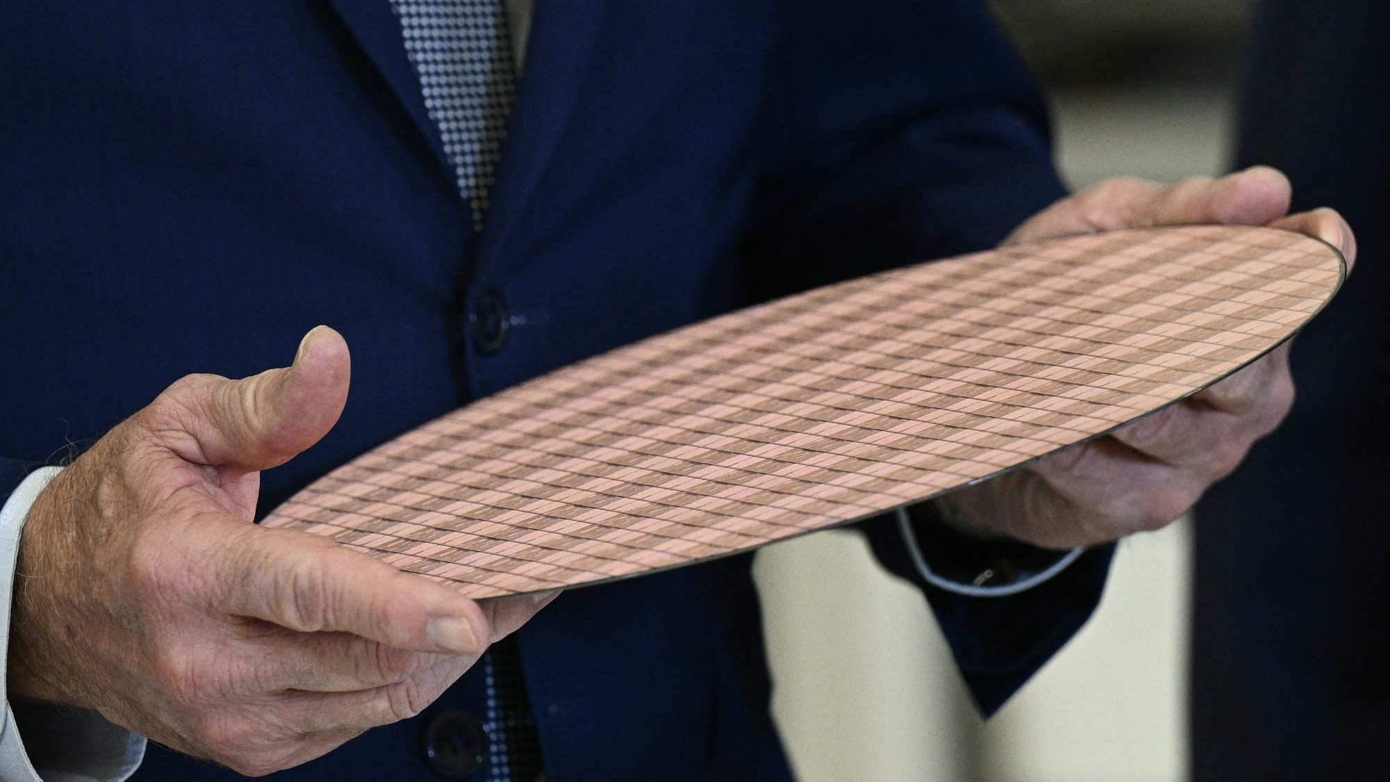
Intel Foundry was established with the goal of directly competing with TSMC and Samsung in contract chip manufacturing. But in the years since its launch in 2021, Intel Foundry has been dominated by delays, customer dropouts, and a brutally honest admission in Intel’s latest filings that Intel Foundry has so far failed to attract significant customers.
Intel previously said its 1.8nm-class 18A process was on track for foundry in 2025 — indeed, risk production began in Q1 — and it continues to build toward 14A beyond that. But internally, Intel now says that 18A’s first and most important customer isn’t some blue-chip hyperscaler or chip startup but rather, Intel itself.
That’s not necessarily a bad thing. Many successful foundries start by proving their nodes with internal products. However, it highlights how far Intel still is from market leaders. TSMC is already producing 3nm chips for Apple and working toward 2nm volume next year. Samsung, despite customer churn, is also advancing its roadmap.
Intel Foundry's biggest problem remains yield. The 18A process still struggles to produce usable chips at high enough rates to be viable at scale, and that cost parity with TSMC is still out of reach. Intel’s own earnings show Intel Foundry losing billions per quarter, with operating losses of more than $3 billion reported for Q2 2025 alone.
Packaging first, foundry later
What Intel has succeeded in doing is packaging, and Lip-Ban Tu knows it. The joint Nvidia-Intel announcement was in many ways framed as a potential packaging breakthrough, with Jensen Huang highlighting Intel’s ability to connect Nvidia’s GPU chiplets with Intel CPUs using Foveros, calling it the kind of multi-technology integration that other foundries simply can’t deliver in the same way.
That packaging capability may well become Intel’s biggest near-term advantage. Foveros and EMIB give the company a mature chiplet integration stack, well-suited to an era where performance gains come more from heterogeneous integration than monolithic scaling. And with Nvidia, Intel finally has a marquee partner willing to bet on that stack, even if not (yet) on the foundry behind it.
There’s another reason Intel is focusing on packaging — it buys time. Unlike bleeding-edge wafer production, packaging doesn’t demand the same kind of node-level maturity. It allows Intel to use proven dies, whether its own or those of its partners, while demonstrating value through integration and system-level efficiency. It also aligns with the broader U.S. industrial strategy, which increasingly sees chip packaging as a national priority.
And because Foveros can integrate chiplets from multiple sources, Intel isn’t locked into its own process nodes. As Huang noted, Nvidia’s chiplets still come from TSMC, but the package doesn’t have to. Intel’s unique cross-foundry packaging model could be a future-proof wedge into multi-vendor systems.
Packaging is also a fast on-ramp for revenue generation for Intel Foundry. Qualifying new chip designs with customers can be a years-long process that takes time to yield revenue and profit, whereas the lead times for chip packaging often only take a few months before revenue generation begins.
A quiet retreat?

Notably, Lip-Bu Tan struck a cautious tone on the company’s foundry ambitions during the joint press conference announcing the Nvidia partnership, saying Intel will continue to qualify its 18A and 14A nodes “one step at a time” before deciding whether to use them for outside customers. Rather than promising a rush of third‑party wafers, he focused on Intel’s advanced packaging technologies — Foveros and EMIB — as the near‑term selling point for the Nvidia collaboration and other potential customers.
That corresponds with Intel’s broader roadmap plans to ship 18A first for its own CPUs, prove the node works, and only then court external foundry clients. According to recent reporting, Intel may even shift its focus toward the upcoming 14A process, which it believes could be more competitive with TSMC than the delayed 18A node.
Meanwhile, Intel is leveraging its U.S. footprint and CHIPS Act subsidies to position itself as the first to bring advanced-node production online within American borders — even as TSMC builds its own 3nm and future 2nm fabs in Arizona. The U.S. government has emerged as a critical early customer, with motivation for funding Intel’s fabs through up to $7.9 billion in federal subsidies to support U.S. government and defense needs. None of that guarantees success, but it gives Intel runway to keep building. And if geopolitical risk around Taiwan grows, or if TSMC struggles to meet overwhelming demand, the mere existence of a second, U.S.-based option may be enough to draw customers back.
Still, the competitive reality is truly stark. Apple, Nvidia, AMD, Broadcom — all these industry leaders build their most important products at TSMC. Even Intel’s closest collaborators are not switching to Intel Foundry wafers. Both Tan and Huang acknowledged that TSMC is a world‑class foundry during the press conference and deferred any talk of deeper manufacturing ties to the future. So, the future of Intel Foundry remains dependent on Intel proving to the market that its chips are worthwhile, as for how that goes? It all remains to be seen.
Follow Tom's Hardware on Google News to get our up-to-date news, analysis, and reviews in your feeds. Make sure to click the Follow button.

Luke James is a freelance writer and journalist. Although his background is in legal, he has a personal interest in all things tech, especially hardware and microelectronics, and anything regulatory.
