Why packaging is a huge part of Nvidia's $5B Intel deal — Foveros could speed up market delivery
Foveros and EMIB are doing more than stacking dies; they’re accelerating Nvidia’s roadmap.

Intel isn’t the most obvious partner for Nvidia. The two companies have competed across consumer, data center, and AI markets for decades with no shortage of friction. But on a joint call on September 18, following news of an unexpected partnership, Nvidia CEO Jensen Huang and Intel chairman Lip-Bu Tan turned that dynamic on its head, announcing that Nvidia will invest $5 billion in Intel and begin using its packaging technology for an upcoming SoC line.
Why? Not for foundry capacity in the traditional sense, and not just to keep a geopolitical hedge against Taiwan. According to Huang, the key factor was packaging. “Intel has the Foveros multi-technology packaging capability,” he said, “and it’s really enabling here… connecting NVIDIA's GPU die chiplet with Intel's CPUs in a multi-technology packaging capability and multiprocess packaging technology.”
Tan agreed. “Foveros and EMIB is [sic] a really good technology,” he added, calling the packaging roadmap “a great opportunity for both of us.” In recent years, packaging has become Intel’s fastest and most reliable on-ramp to foundry revenue. For Nvidia, that makes it the shortest path to market for its next-generation AI SoCs and the likely primary driver behind the partnership.
Why the attraction to Intel’s packaging?
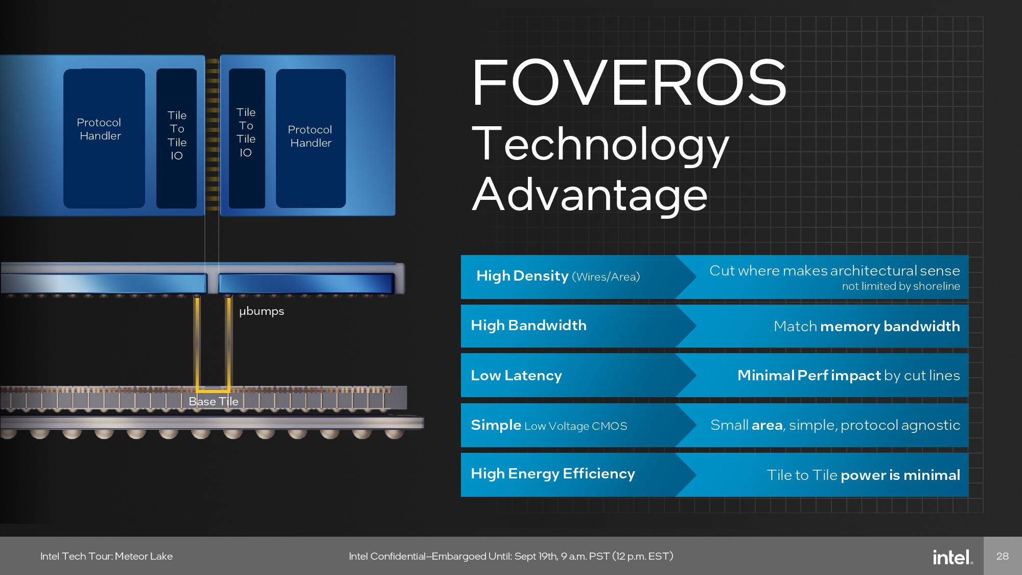
The packaging that Huang praised by name — Foveros — is Intel’s 3D chip stacking solution. Unlike traditional multi-die packages, which spread chiplets side-by-side on a shared substrate, Foveros stacks one directly on top of another using through-silicon vias (TSVs). This shortens interconnect length and offers significantly higher bandwidth than planar layouts. It also allows each tile in the stack to be built on a different process node, enabling designers to assign logic to the most appropriate tech for performance or cost.
If Foveros is the vertical axis of Intel’s packaging portfolio, EMIB (Embedded Multi-die Interconnect Bridge) is the horizontal one. EMIB embeds thin silicon bridges inside the package substrate to link dies together at a high density and low power without the need for a massive silicon interposer. More recently, Intel has combined the two in what it calls Co-EMIB: Foveros stacks linked together across a package using EMIB bridges.
What this all adds up to is a system for building complex chiplet-based products that behave more like monolithic SoCs, and Intel has spent the better part of a decade turning it into a viable business. Intel's Ponte Vecchio GPU used Foveros and EMIB. So did Meteor Lake. And crucially, Intel has been manufacturing these packages at volume. The company’s $3.5 billion Foveros-capable facility in New Mexico went live last year, giving Intel the domestic capacity to court U.S. AI and cloud players looking to hedge their reliance on overseas providers.
The fastest on-ramp to foundry revenue

Intel has increasingly positioned advanced packaging as a central pillar of its foundry strategy due to its near-term business upside. During its Direct Connect event back in April, the company highlighted packaging alongside manufacturing capacity and ecosystem development as core to its customer-first push, emphasizing how Foveros and EMIB allow Intel Foundry to serve heterogeneous compute needs without requiring customers to wait on new process nodes.
We described Intel's packaging breakthroughs earlier this year as “the fastest on-ramp to meaningful revenue generation,” particularly when compared to the long ramp cycles associated with new front-end process technologies.
This framing was echoed by Huang during the joint call. “In the case of our consumer PC, we will sell… Nvidia’s GPU chiplet… to Intel,” he said, adding, “And that is then packaged into an SoC.” That chiplet will be bonded using Foveros or Co-EMIB and then shipped as part of a complete product.
In other words, Nvidia gets to leverage Intel’s infrastructure and packaging stack without waiting for its core foundry nodes to catch up. That might be the entire point. Nvidia’s highest-volume AI parts now use chiplet designs with extreme interconnect and bandwidth demands. Intel’s packaging lets Nvidia skip the wait by integrating existing GPU dies with new CPU tiles — a point Huang hammered home repeatedly. “... It’s really a fabulous way of mixing and matching technology… that's… why we're going to be able to innovate so quickly and build these incredibly complex systems,” he said.
Tan echoed the sentiment. “I think it’s a great opportunity for both of us,” he said. “... We will definitely continue to refine it [Foveros and EMIS] and make sure [that it’s] reliable and the yield [improves].”
A fast path to yield optimization
Unlike bleeding-edge nodes, which can easily be bottlenecked, Intel’s advanced packaging offers Nvidia a fast path to yield optimization and market delivery. With U.S. demand for AI systems surging, Nvidia needs a second-source capacity that isn’t located entirely in Taiwan. Intel provides that, with domestic packaging and a fast-maturing foundry model built around chiplet assembly.
But geography aside, the partnership is ultimately about what Intel’s packaging lets Nvidia do that no one else can deliver on the same timeline: Build hybrid, multi-chiplet SoCs with custom CPUs, GPU dies from another fab, and ultra-high-bandwidth interconnect between them. That’s not a TSMC job, nor is it a Samsung one. It’s exactly the kind of complex system Intel’s packaging team has been preparing for years, and now it has Nvidia as its highest-profile customer.
Follow Tom's Hardware on Google News, or add us as a preferred source, to get our up-to-date news, analysis, and reviews in your feeds. Make sure to click the Follow button!

Luke James is a freelance writer and journalist. Although his background is in legal, he has a personal interest in all things tech, especially hardware and microelectronics, and anything regulatory.

