Intel Announces 48-Core Cascade Lake-AP, Xeon E-2100 Processors (Update)
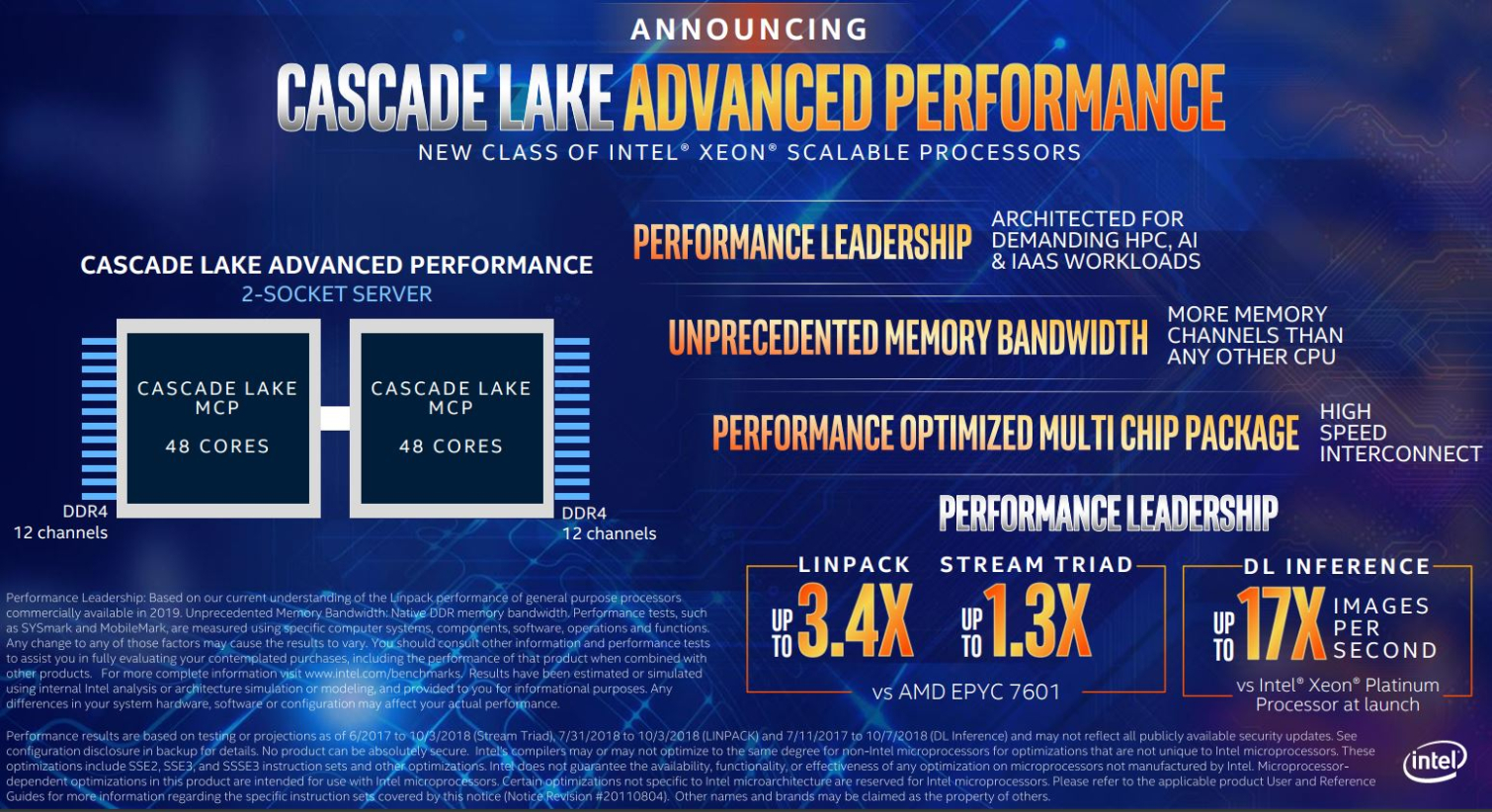
Intel made a few announcements ahead of the pending Supercomputer 2018 trade show, including its new family of Xeon Cascade Lake-AP (Advanced Performance) processors that come with up to 48 cores and support for 12 channels of DDR4 memory.
Intel designed this new lineup of data center chips with a Multi-Chip Package (MCP) architecture, meaning each processor is composed of several dies, much like AMD's EPYC and Threadripper processors. That finally gives Intel an answer to AMD's core count advantage that it holds with its 32-core EPYC data center processors. Intel also announced a new lineup of Xeon E-2100 processors for entry-level servers.
Intel Xeon Cascade Lake-AP (Advanced Performance)
The Cascade Lake-AP family marks a fundamental shift in Intel's data center processor design, although the company took a philosophically similar approach with the Kentsfield processors. This new family of processors comes with up to 48 cores per chip and supports 12 DDR4 channels, making up to 96 cores and 24 DDR4 channels available in a dual-socket (2P) server. Intel hasn't confirmed if the processors feature Hyper-Threading, which would equate to 96 threads per chip.
Intel claims the processors offer the highest-performance available for HPC, AI, and IAAS workloads. The processors also offer the most memory channels, and thus access to the highest memory bandwidth, of any data center processor. Performance density, high memory capacity, and blistering memory throughput are the goal here, which plays well to the HPC crowd.
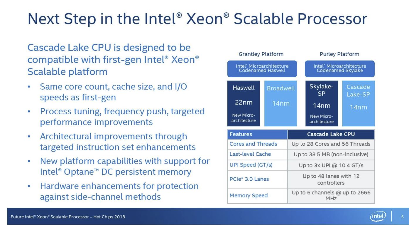
As a quick refresher, the Xeon Cascade Lake-SP series is coming to market soon. Intel hasn't released specific details of the models, but we do know the new processors will come bearing the same basic design as the Intel Xeon Scalable Processors (review here). That means Cascade Lake is another 14nm refresh with similar core counts (up to 28), cache capacities, and I/O accommodations as the previous-gen models.
Those new Cascade Lake-SP models come to market this year, leaving Intel to compete with AMD's 32-core EPYC processors that have more cores and threads at their disposal. AMD has also been vocal that it's 7nm EPYC processors, which will purportedly come with even more cores, are on track for shipment for revenue early next year.
Potentially ceding both process and performance leadership to AMD would set the stage for a long 2019 as Intel awaits the 10nm Ice Lake data center processors in 2020, hence the debut of the exotic Cascade Lake-AP processors.
Get Tom's Hardware's best news and in-depth reviews, straight to your inbox.
Intel claims the new Cascade Lake-AP processors beat the flagship AMD EPYC 7601 in the following benchmarks. Intel used publicly available AMD test results for the Steam Triad results, but conducted the Linpack tests in its labs. Intel chose to disable SMT on the EPYC 7601, thus disabling half its threads. We've reached out to Intel for the rationale behind the test configuration (EDIT - We've included Intel's comments at the end of the article).
· Linpack up to 1.21X versus Intel Xeon Scalable 8180 processor and 3.4X versus AMD EPYC 7601
· Stream Triad up to 1.83X versus Intel Scalable 8180 processor and 1.3X versus AMD EPYC 7601
Intel also claims the processors offer up to 17X more AI/Deep Learning inference performance than its Xeon Scalable 8180 did at launch.
Gluing Together the Die
We expect all of the architectural improvements of the -SP models to work their way into the new Cascade Lake-AP models. But the addition of an MCP (Multi-Chip Package) design is, while in line with Intel's recent statements that multi-chip architectures are part of its path forward, surprising in light of statements the company made about AMD's multi-chip EPYC design in the past.
Intel famously claimed the EPYC design consisted of "four glued-together desktop die." (The statement referred to the technical term "glue logic," which in AMD's case is the Infinity Fabric.) Intel decries AMD's multi-chip approach as offering inconsistent performance (among other perceived faults).
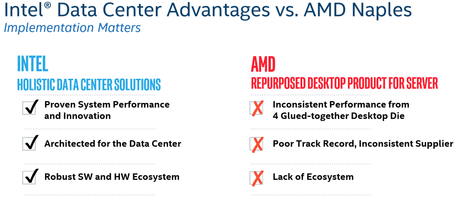
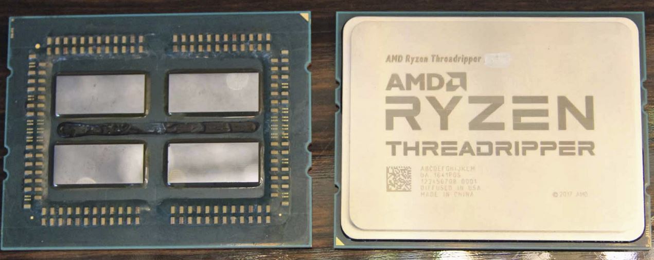
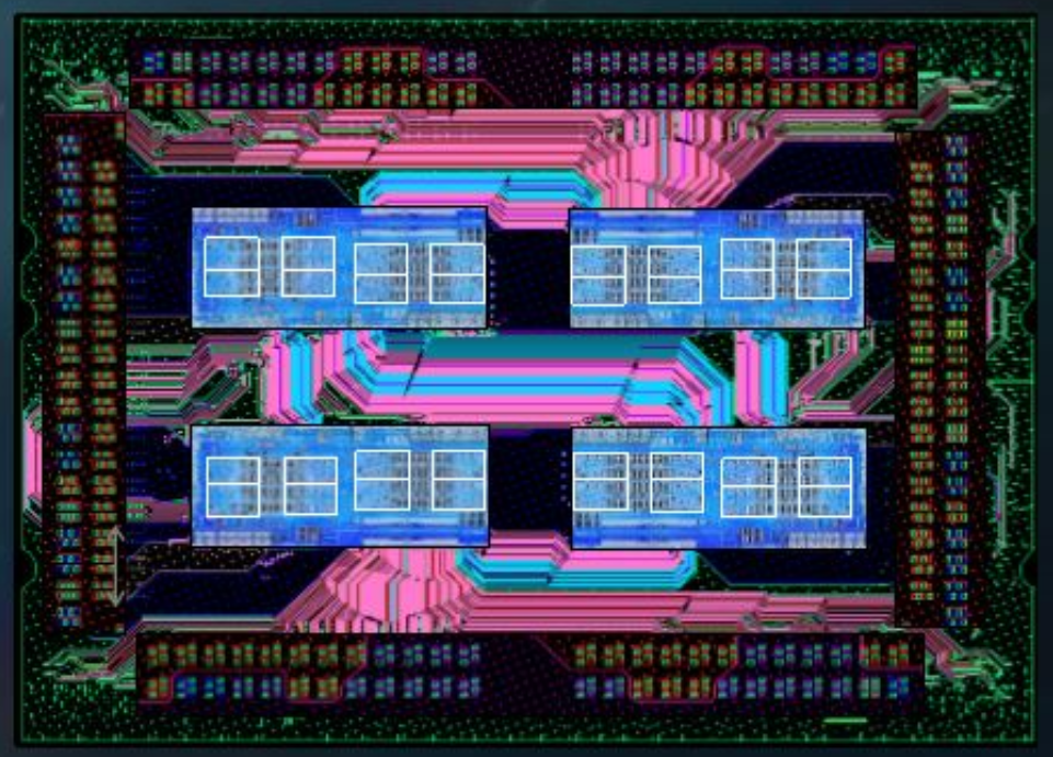
When asked the difference between its approach and AMD's, Intel representatives responded that the company does not "object" to multi-chip designs. Instead, it sees value in a path that it already takes with its SOCs. Intel also claims its design is superior to AMD's Infinity Fabric-based architecture (pictured above).
Intel contends AMD's approach creates inconsistency and performance variability, while its design will not suffer from the same eccentricities. Intel is using its UPI (Ultra Path Interconnect) interface between the die inside the package. This protocol is extremely scalable; Intel already uses it to communicate between processors in up to eight-socket servers, so it obviously has the correct accommodations for complex topologies, along with mature scheduling and power-saving algorithms.
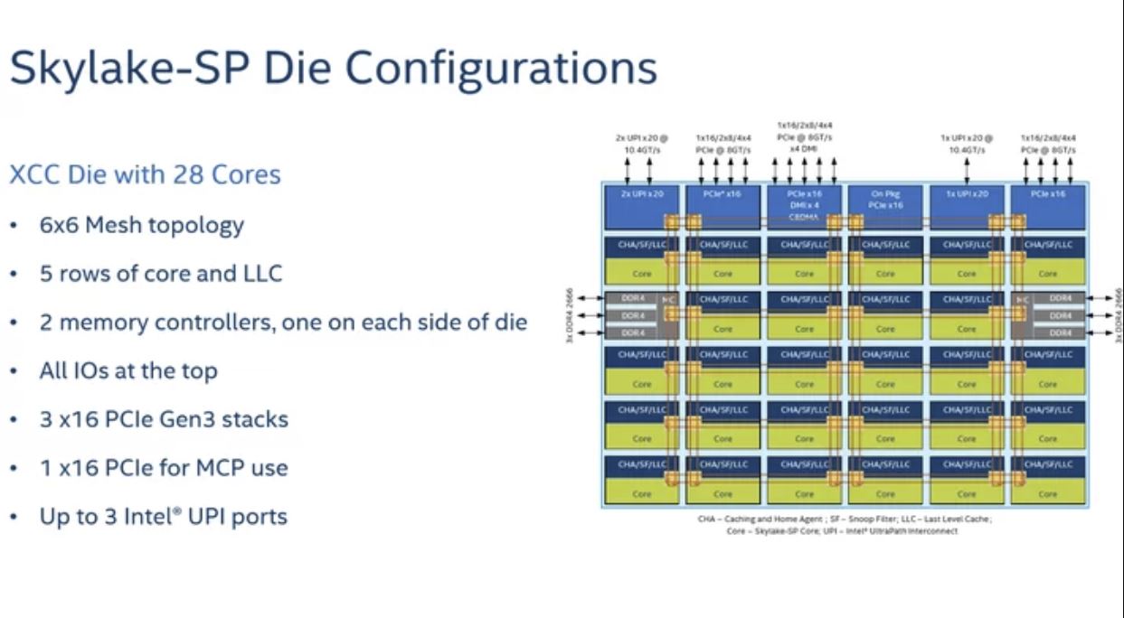
UPI is also already built into Intel's Xeon Scalable XCC die, as seen above. Each die has three UPI connections for communication with processors (and their attached memory) resident on other sockets. It would make sense to use the third existing UPI port for communication between dies within the same processor package, while leaving the other two UPI connections free for the connection to the other processor in a two-socket server.
Intel will likely separate the disparate pools of resources inside each -AP processor with either NUMA or some type of advanced Sub-NUMA Clustering (SNC). Think of this as a quad (or more) socket topology within a dual-socket server.
Intel says that the Cascade Lake-AP models will only scale to two sockets, as opposed to the eight-socket scalability found with the flagship Xeon processors, so it's logical to assume that Intel has simply made sophisticated adjustments to its existing XCC die to accommodate a multi-chip design. Each Cascade Lake-AP chip also wields 12 memory channels, which aligns nicely with combining two six-channel XCC dies into a single package.
But Intel hasn't confirmed the chip only comes with two dies, and the Cascade Lake-AP models only come with up to 48 cores. That means the company may have designed an entirely new die or disabled four cores per 28-core XCC die to fit within thermal limitations. Intel did reveal that it isn't using an EMIB connection between the dies, likely due to thermal expansion and contraction between the power-hungry dies, but did not provide additional detail on the interconnect.
Intel isn't releasing concrete details, including whether these processors will require a new socket (they are rumored to drop into an LGA5903 socket). We expect Intel will release multiple SKUs that span the core-count gap between its 28-core -SP models and the 48-core -AP flagship.
We also know that Intel isn't averse to charging a premium for its "performance leadership" products, and with current-gen 28-core Xeons carrying a recommended customer price of $10,000 for a single processor, these will likely come with a steep price tag. Intel hasn't disclosed pricing yet, but the firm stated the new processors would be available in the "first part" of 2019.
Intel Xeon E-2100 series
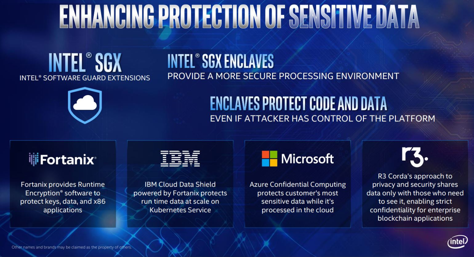
Intel also announced Xeon E-2100 series of processors. These processors come bearing the same fundamental design as the Xeon E processors the company released earlier this year for workstations, but Intel designed the new additions for entry-level servers. That makes them a good fit for small-to-medium sized businesses. Intel also added support for its latest SGX technology, which cloud service providers like Microsoft and IBM use to secure data in the cloud.
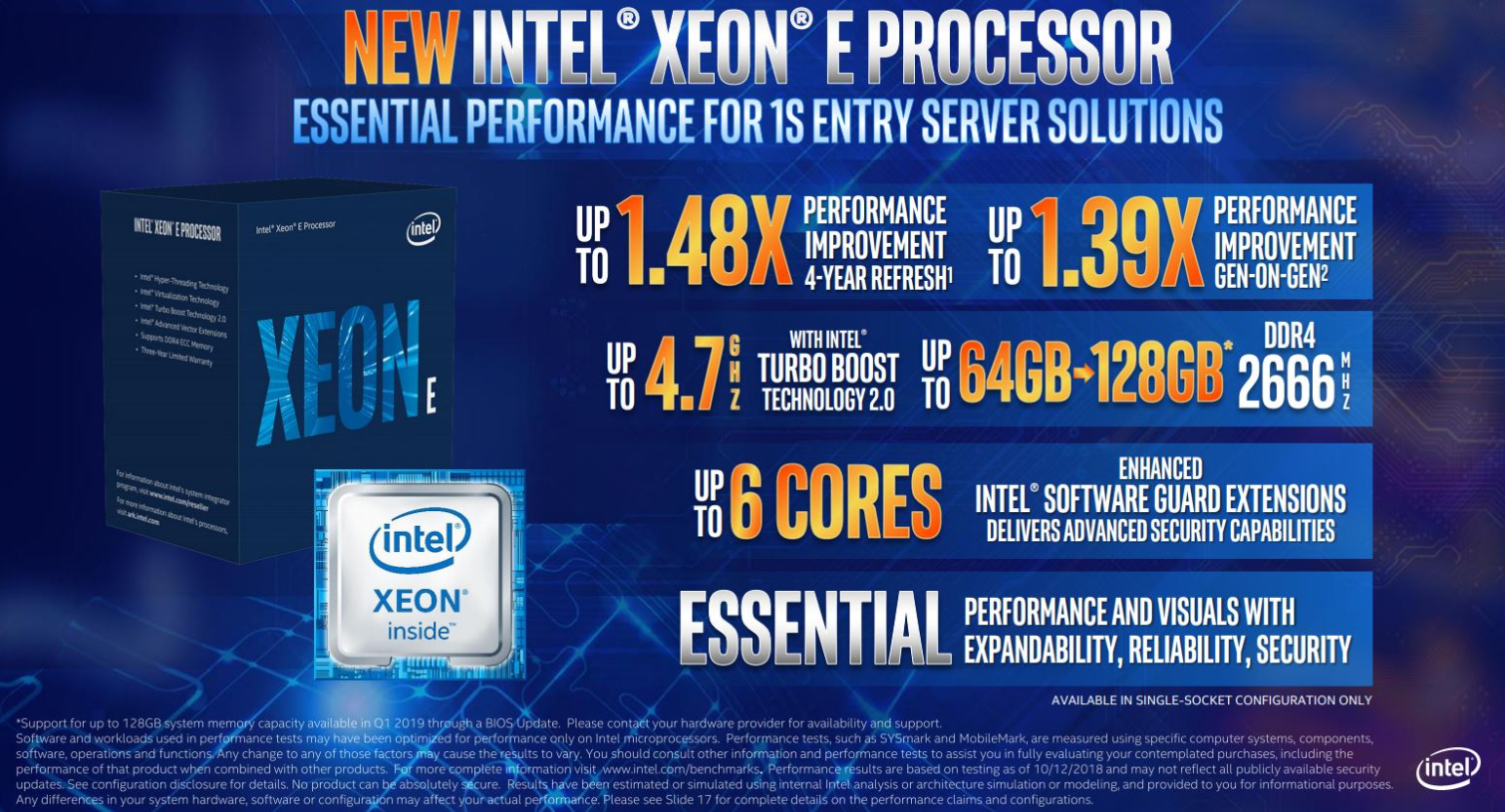
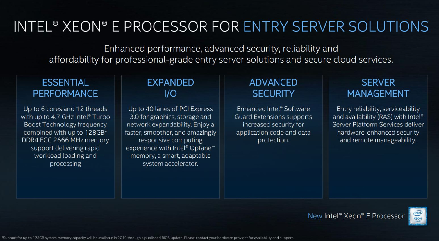
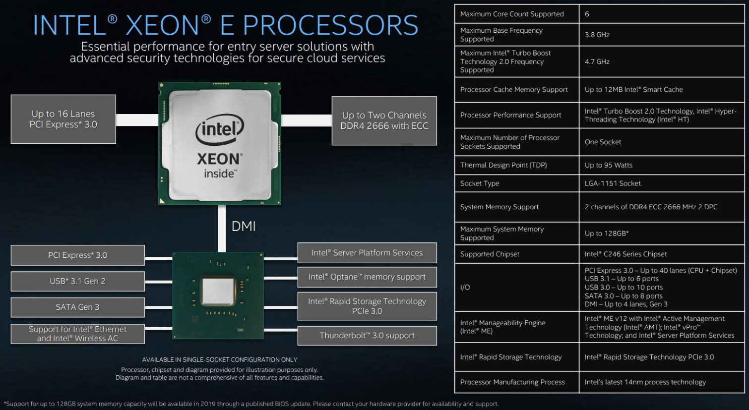
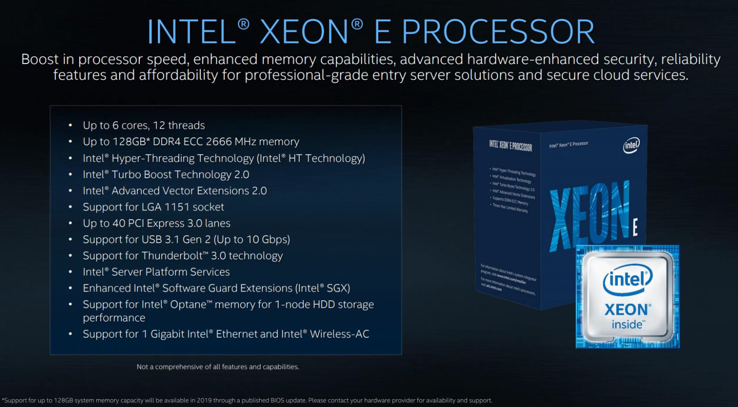
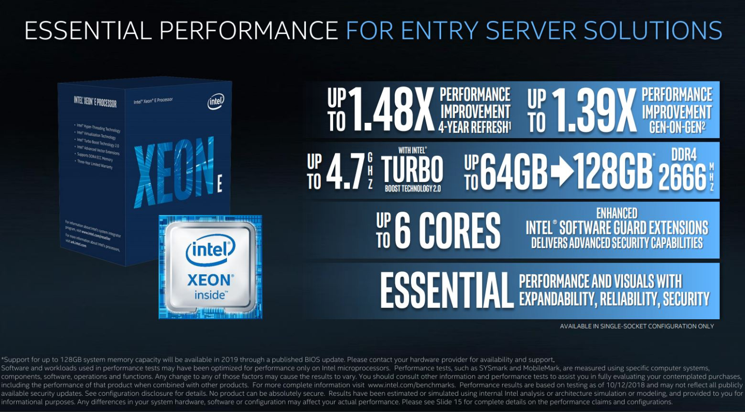
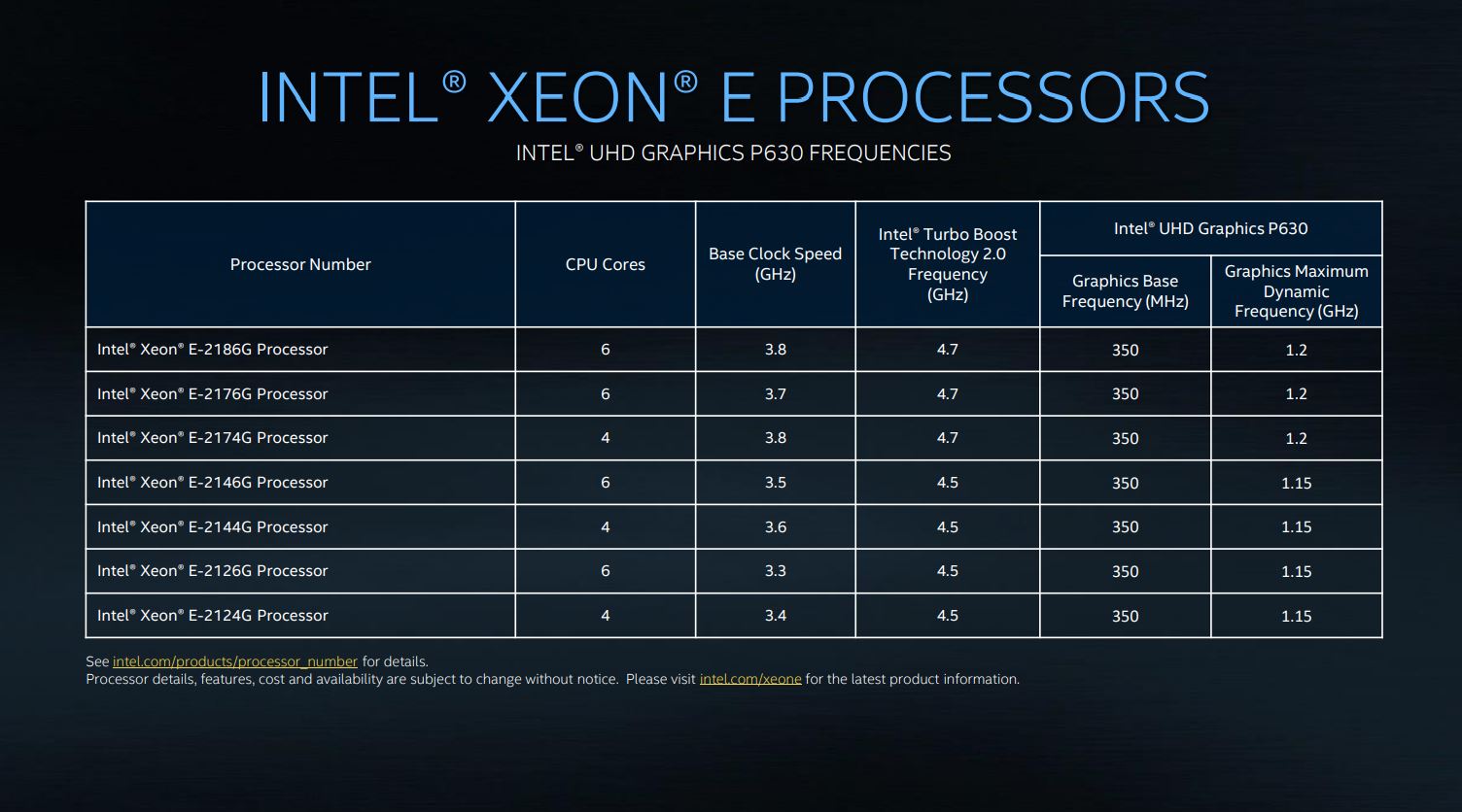
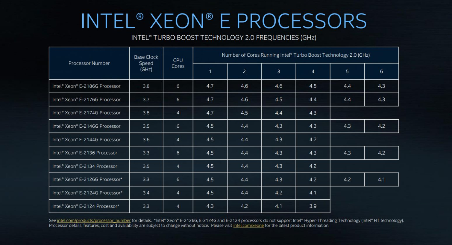
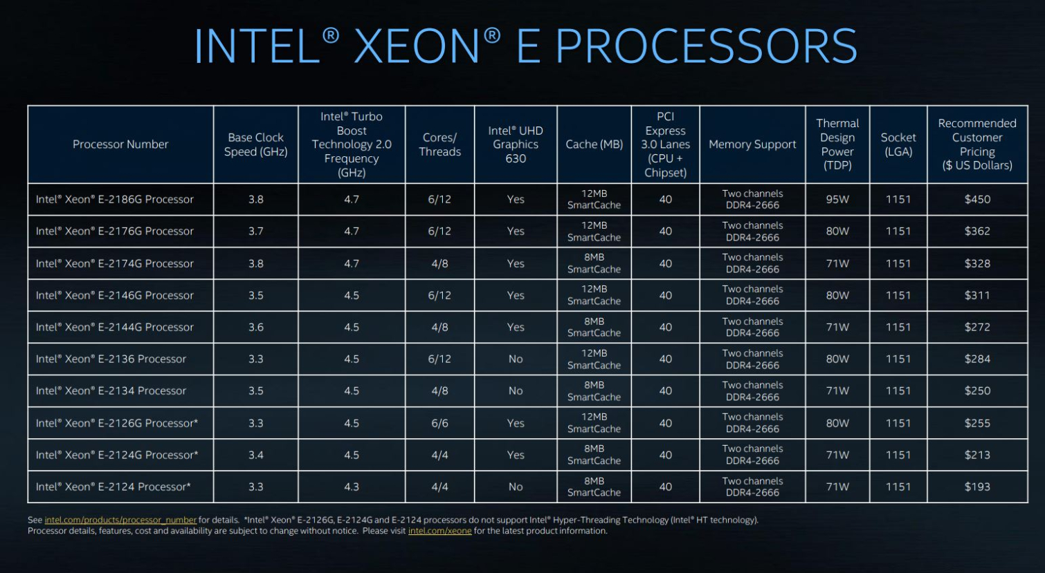
Intel built the new processors with the same fundamental design as its Coffee Lake processors and are available in SKUs that range from four cores and four threads up to six cores and 12 threads, but the Xeon E models support up to 40 PCIe Gen 3.0 lanes. Intel splits the lanes between 16 lanes exposed to the user and four DMI 3.0 lanes that connect to the C246 workstation-series chipset that provides an additional 24 usable lanes.
The processors drop into the LGA1551 socket and come outfitted with a dual-channel memory controller and supports up to 128GB of DDR4-2666 ECC memory (double the capacity of the workstation models). With the exception of the E-2124, all of Intel's new E-2100 models come with a "G" modifier, meaning they come equipped with an integrated UHD Graphics P630 engine. TDP's range from 71W to 95W.
The Xeon E-2100 series processors are available today.
UPDATE: Intel disabled Simultaneous Multi-Threading (SMT) on AMD's EPYC processor for its performance comparisons, disabling half the threads on the chip. Intel responded to our queries about the settings:
It’s common industry practice for us to disable simultaneous multithreading on processors when running STREAM and LINPAK to achieve the highest performance, which is why we disabled it on all processors we benchmark.
We reviewed Intel's in-house performance benchmarks of the same EPYC 7601 processor that it shared with us earlier this year, and the company did not disable SMT for those Stream tests. Instead, the company assigned the test to execute with one thread per core, which serves the same purpose as disabling SMT.

Paul Alcorn is the Editor-in-Chief for Tom's Hardware US. He also writes news and reviews on CPUs, storage, and enterprise hardware.
-
Blas I wonder why this announcement was made today, Nov the 5th. It probably has nothing to do with the fact that tomorrow, on Nov the 6th, AMD is holding its "Next Horizon" event to introduce the new 7 nm Zen 2 architecture. Probably. Although i'm guessing someone at Intel's marketing department has had to spend the weekend preparing these few slides :)Reply -
bit_user Reply
And yet still probably less than Nvidia's Tesla T40, which likely costs only 10% or 20% as much and burn far less power (50 - 75 W each).21458221 said:Intel also claims the processors offer up to 17X more AI/Deep Learning inference performance than its Xeon Scalable 8180 did at launch.
Perhaps two of each die's UPI links are to each other, with one link each going to the outside. But I guess you could have a total of 4 links going to the outside for a fully-connected topology between all 4 dies in a 2-socket config. I just think it would scale better to have more connectivity between dies in-package, given that a single UPI link would probably still be a choke point for apps requiring substantial die-to-die communication.21458221 said:It would make sense to use the third existing UPI port for communication between dies within the same processor package, while leaving the other two UPI connections free for the connection to the other processor in a two-socket server.
Wow, that's a surprising indictment against EMIB. Quite a reversal, given how hard they were pushing it even within the past year.21458221 said:Intel did reveal that it isn't using an EMIB connection between the dies
For 12 memory channels, I imagine they must.21458221 said:whether these processors will require a new socket (they are rumored to drop into an LGA5903 socket)
I wonder how many PCIe lanes they'll support. Dare we hope to see all 96 lanes per socket?
These look to be nothing more than the Xeon flavor of the Coffee Lake desktop CPUs introduced about a year ago. This uncharacteristically long lag - normally it's >= 6 months, IIRC. I might be interested in a Xeon version of the i9 9900K, but I guess that might take another year...21458221 said:Intel also announced Xeon E-2100 series of processors. -
redgarl Reply21459565 said:I wonder why this announcement was made today, Nov the 5th. It probably has nothing to do with the fact that tomorrow, on Nov the 6th, AMD is holding its "Next Horizon" event to introduce the new 7 nm Zen 2 architecture. Probably. Although i'm guessing someone at Intel's marketing department has had to spend the weekend preparing these few slides :)
In catastrophe... and with unverifiable number.
-
JamesSneed Im guessing this 48 core cpu will cost 15-20K if we extrapolate out per core pricing from the 28 core pricing.Reply -
Olle P Reply... Intel hasn't confirmed the chip only comes with two dies, ... That means the company may have designed an entirely new die or disabled four cores per 28-core XCC die
Why not 3x18 or 4x12 cores?
No matter which it will either suck a lot of power or run at a really low speed.
Absolutely Preposterous!21459524 said:AP = Additional Profit edition?
-
Grzegorz Wereszko Fine print. 48 core vs 32 core Epyc (with SMT disabled)... so good work Intel.. . Guessing that they didn't learn from their recent i9 9900k review?Reply -
omniphonix I wonder if Intel's interposer design solves the problem AMD has with low-latency applications on multi-die packages.Reply
http://www.scanproaudio.info/2018/08/24/threadrippers-2990wx-2950x-on-the-bench-just-a-little-bit-of-history-repeating/
