Intel Xeon Platinum 8176 Scalable Processor Review
Why you can trust Tom's Hardware
The Mesh Topology & UPI
The Scalable Processor family features fundamental changes to the web of interconnects that facilitate intra-processor and inter-socket communication. We covered Skylake-X's topology in Intel Introduces New Mesh Architecture For Xeon And Skylake-X Processors. We also followed up in our Core i9-7900X review with more details, adding fabric latency and bandwidth tests to our analysis. More recently, though, Intel gave us extra info to flavor our take on the mesh.
The Old Way
Processor interconnects move data between key elements, such as cores, memory, and I/O controllers. Several techniques have been used over the years for intra-processor communication. Intel's ring bus served as a cornerstone of the company's designs since Nehalem in 2007. Unfortunately, the ring bus cannot scale indefinitely; it becomes less viable as core counts, memory channels, and I/O increase.
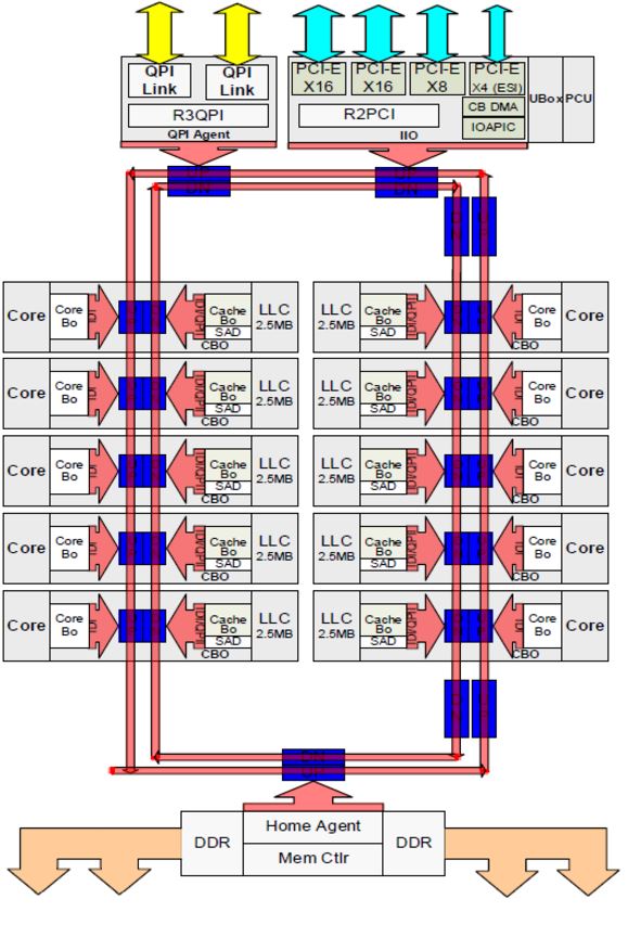
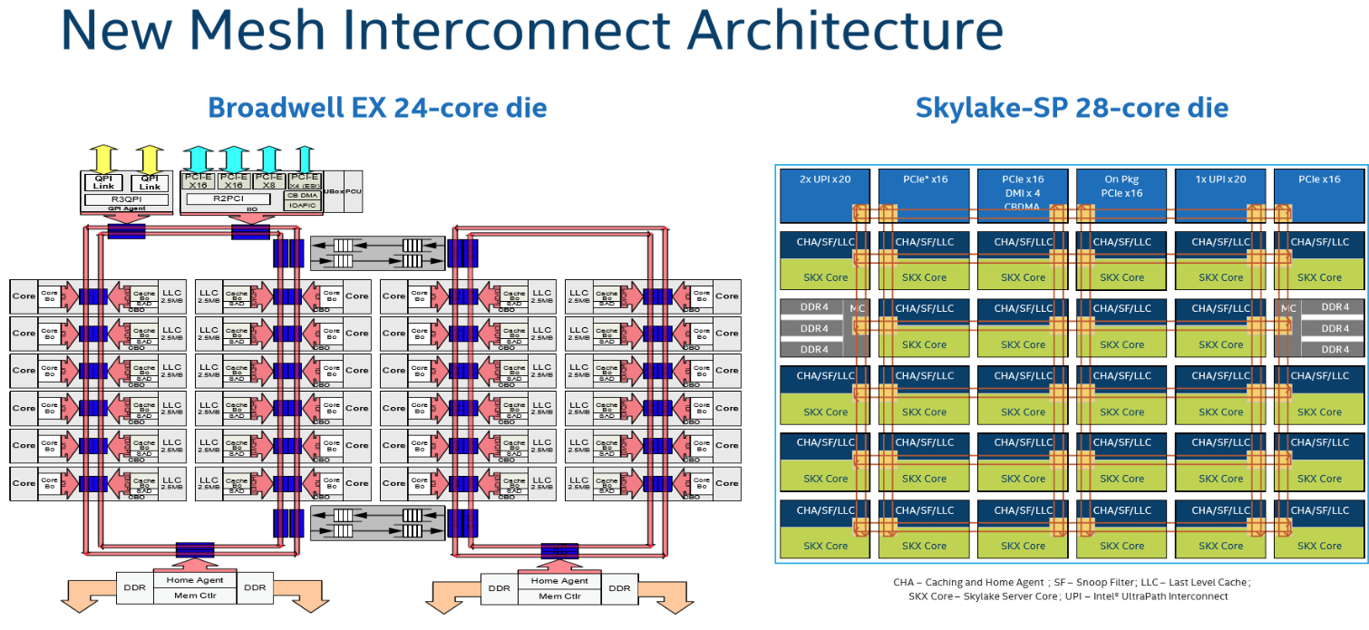
With the ring bus, data travels a circuitous route to reach its destination. As you might imagine, adding stops on the bus amplifies latency. At a certain point, Intel had to split its larger die into two ring buses to combat those penalties. That created its own scheduling complexities, though, as the buffered switches facilitating communication between the rings added a five-cycle penalty.
In the second slide, you can see Intel's mesh topology compared side-by-side to Broadwell-EX's dual ring bus design.
Enter The Mesh
Intel's 2D mesh architecture made its debut on the company's Knights Landing products. Those processors feature up to 72 cores, so we know from practice that the mesh is scalable.
For Skylake-SP, a six-column arrangement of cores would have necessitated three separate ring buses, introducing more buffered switches into the design and making it untenable. Instead, the mesh consists of rows and columns of bi-directional interconnects between cores, caches, and I/O controllers.
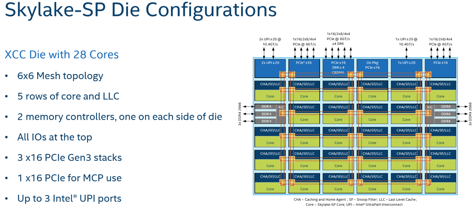
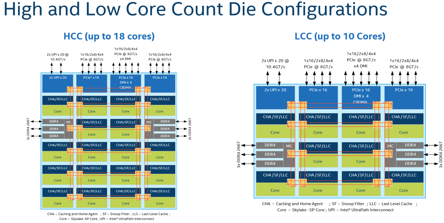
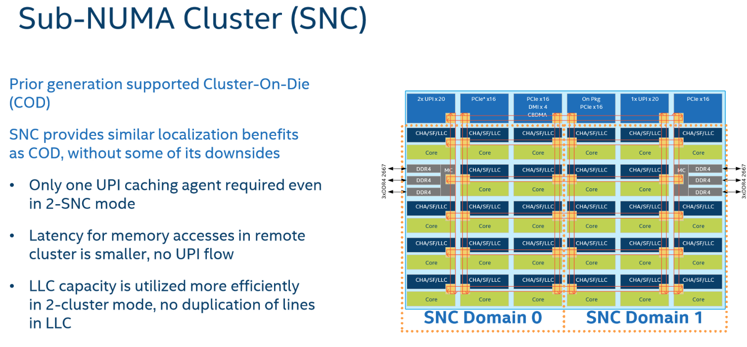
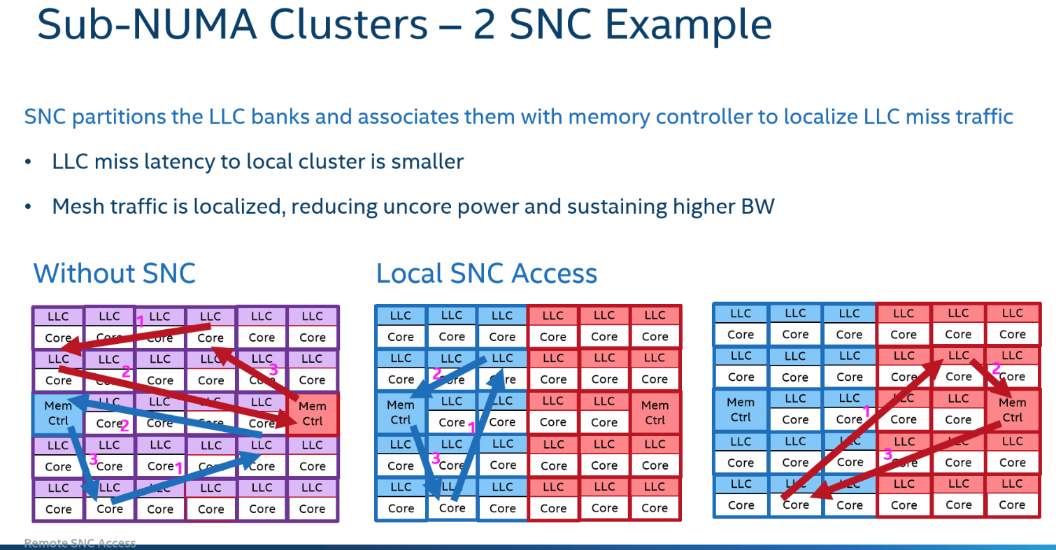
As you can see, the latency-killing buffered switches are absent. The ability to stair-step data through the cores allows for much more complex, and purportedly efficient, routing.
Get Tom's Hardware's best news and in-depth reviews, straight to your inbox.
Intel claims its 2D mesh features a lower voltage and frequency than the ring bus, yet still provides higher bandwidth and lower latency. The mesh operates between ~1.8 - 2.4 GHz to save power, though that figure varies based on the model. Of course, this allows the company to dedicate more of its power budget to completing useful work without sacrificing intra-die throughput. After all, mesh bandwidth also affects memory and cache performance.
Intel constructs its Xeon Scalable Processors from different dies made up of varying core configurations. The XCC (extreme core count) die features 28 cores, the HCC (high core count) arrangement has 18 cores, and the LCC (low core count) implementation has ten. Intel isn't sharing transistor counts or die sizes at this time.
The columns of cores are mirror images of each other with mesh pathways running along the right and left sides of the mirrored cores. This influences the distance between every other column of cores, which translates to more cycles required for horizontal data traversal. For instance, it requires one hop/cycle to move data vertically to the next core's cache, but moving horizontally from the second column to the third column requires three cycles. Intel's Sub-NUMA Clustering (SNC) feature can split the processor into two separate NUMA domains, reducing the latency impact of traversing the mesh to cores/cache farther away. This is similar to the Cluster On Die (COD) tactic Intel used to bifurcate two ring buses on Broadwell-EP processors. SNC provides increased performance in some scenarios, but Intel says it isn't as pronounced with the mesh architecture.
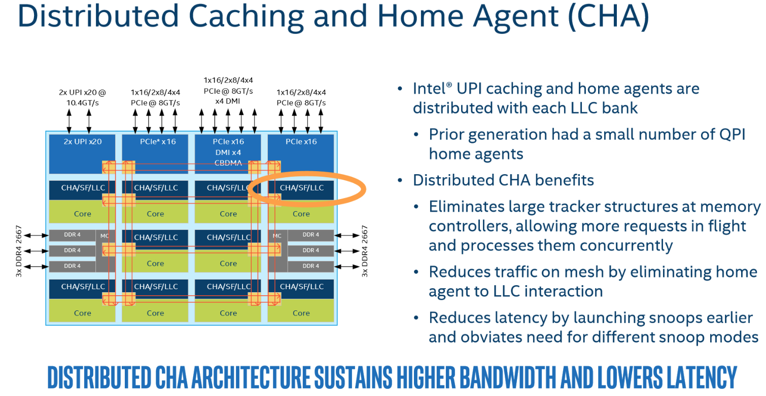
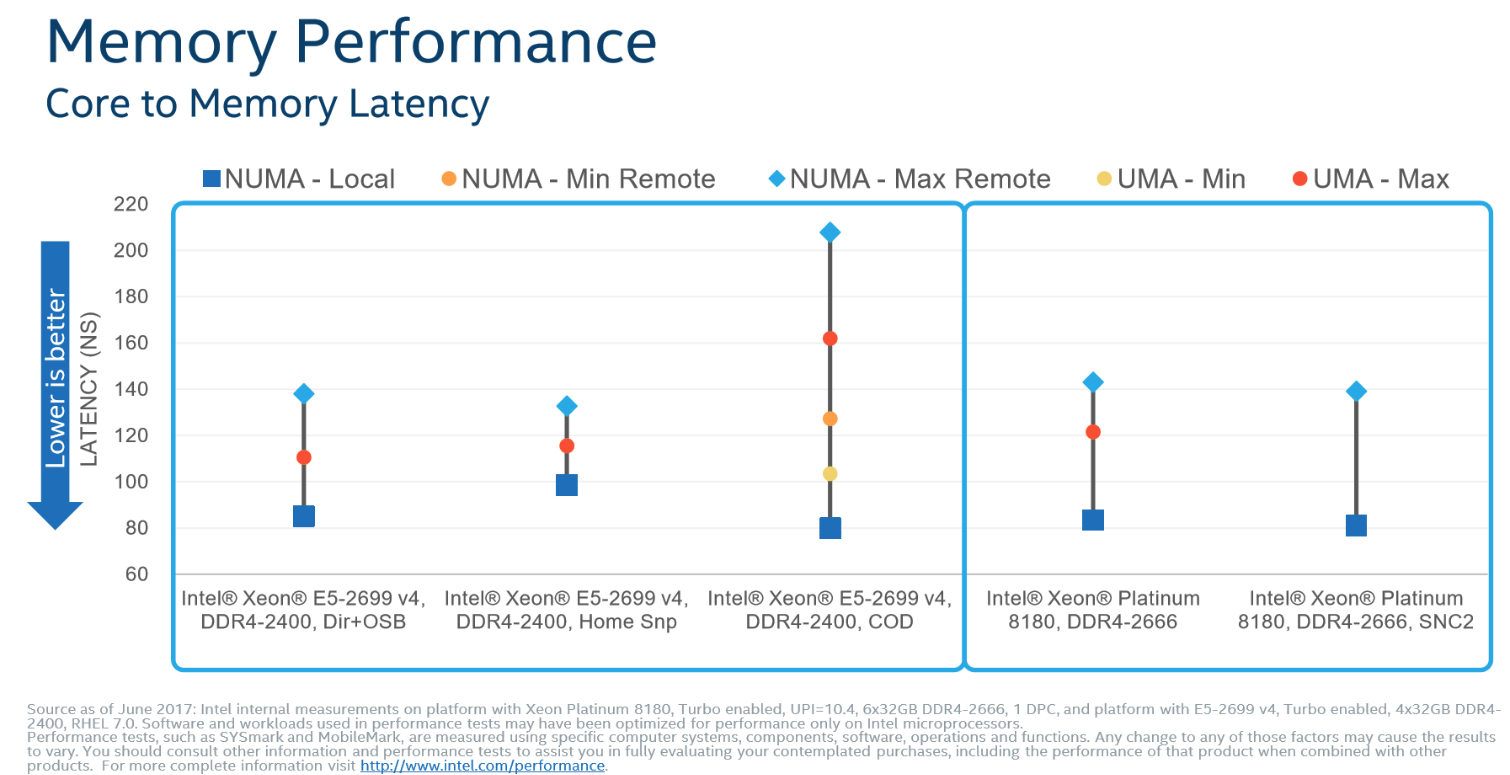
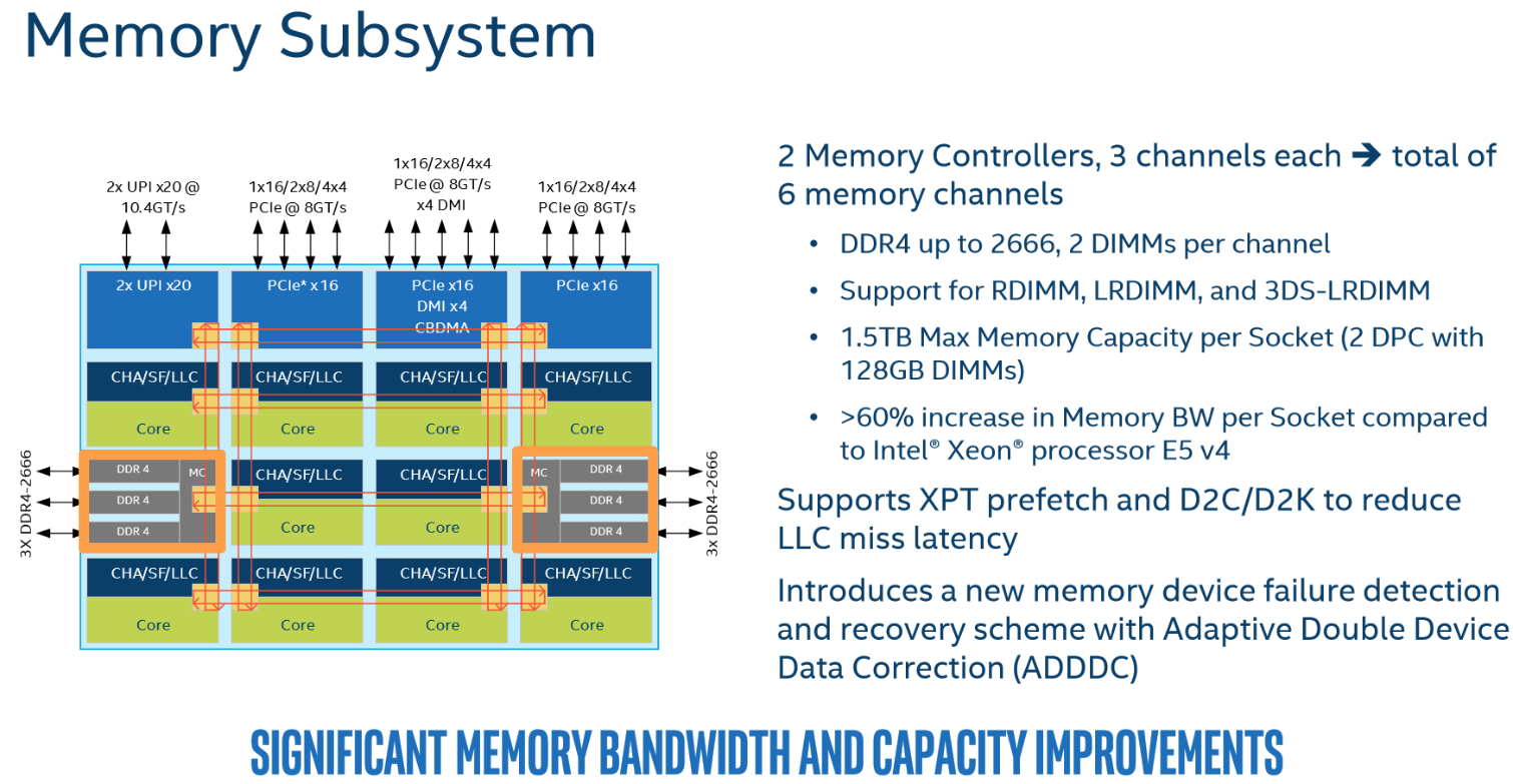
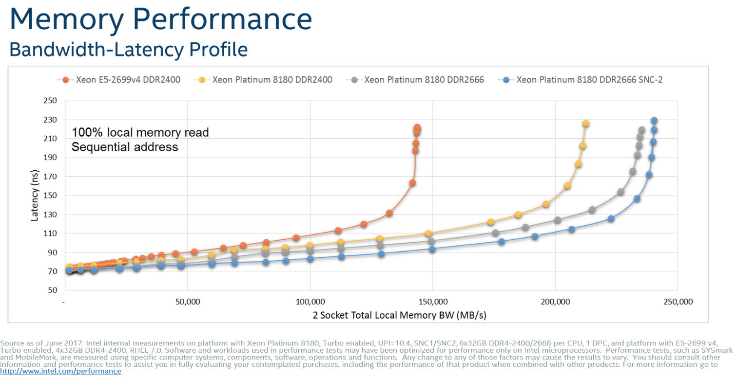
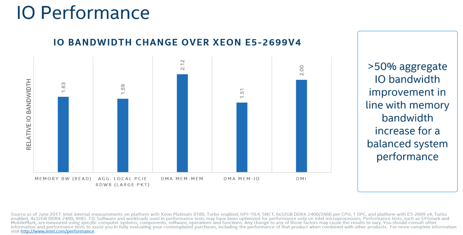
In the past, the caching and home agent (CHA) resided at the bottom of each ring. Intel changed the CHA to a distributed design to mirror the distributed L3 cache. This helps minimize communication traffic between the LLC and home agent, reducing latency.
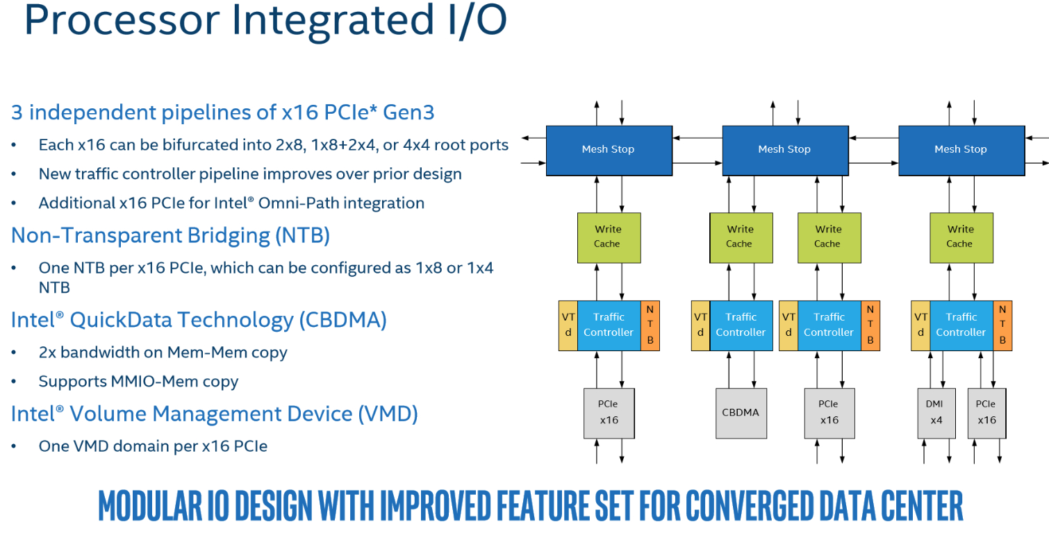
With the Broadwell design, all PCIe traffic flowed into the ring bus at a single point, creating a bottleneck. In Skylake, Intel carves the integrated I/O up into three separate 16-lane PCIe pipelines that reside at the top of different columns (totaling 12 root ports). The modular design provides multiple points of entry, alleviating the prior choke point. Along with other improvements, that provides up to 50% more aggregate I/O bandwidth. Two UPI links also share a single entry point at the top of a column. Models with a third UPI link have an additional entry point. Integrated Omni-Path models also feature an additional dedicated x16 PCIe link, so the networking addition doesn't consume any of the normal lanes exposed to the user.
Intel moved its two memory controllers, armed with three channels each, to opposing sides of the die. You can populate up to two DIMMs per channel (DPC). The 2DPC limitation is a step back from Broadwell's 3DPC support, but of course Intel offsets that with 50% more total channels. You can slot in up to 768GB of memory with regular models or 1.5TB with "M" models. Notably, Intel doesn't impose a lower data rate if you install more DIMMs per channel (1DPC, 2DPC). In contrast, Broadwell processors slowed memory transfers as you added modules to a given channel. That created performance/capacity trade-offs.
Overall, Intel's memory subsystem enhancements provide a massive gain to potential capacity and practical latency/throughput, as we'll see in our tests.
Ultra Path Interconnect (UPI)
The new Ultra Path Interconnect (UPI) replaces the QuickPath Interconnect (QPI). Intel optimized its pathway between nodes because per-socket memory and I/O throughput were increasing so drastically, reaching the limits of QPI's scalability. As with most interconnects, the company could have simply increased the QPI's voltage and frequency to enable faster communication, but still would have faced a point of diminishing returns.
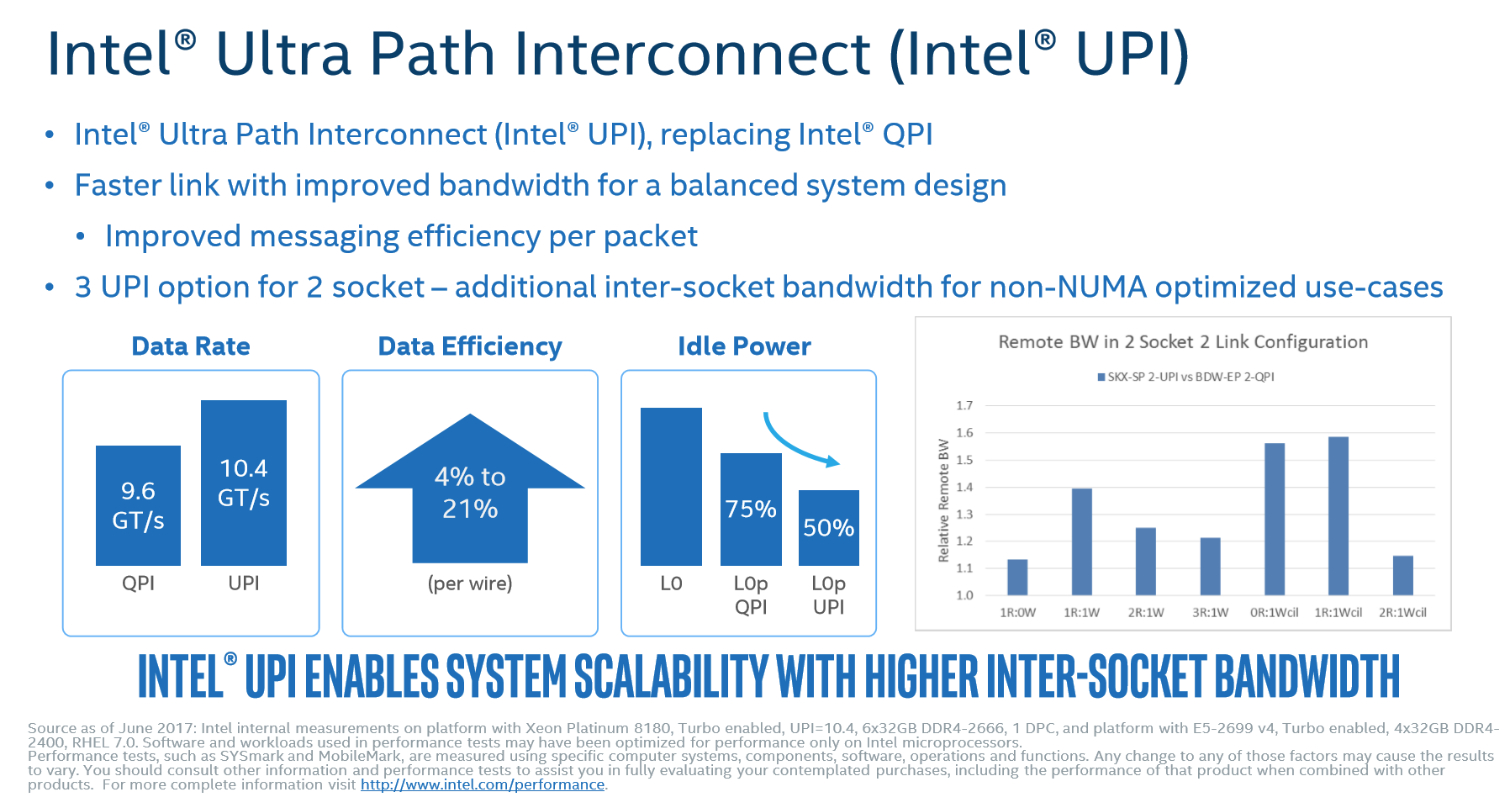
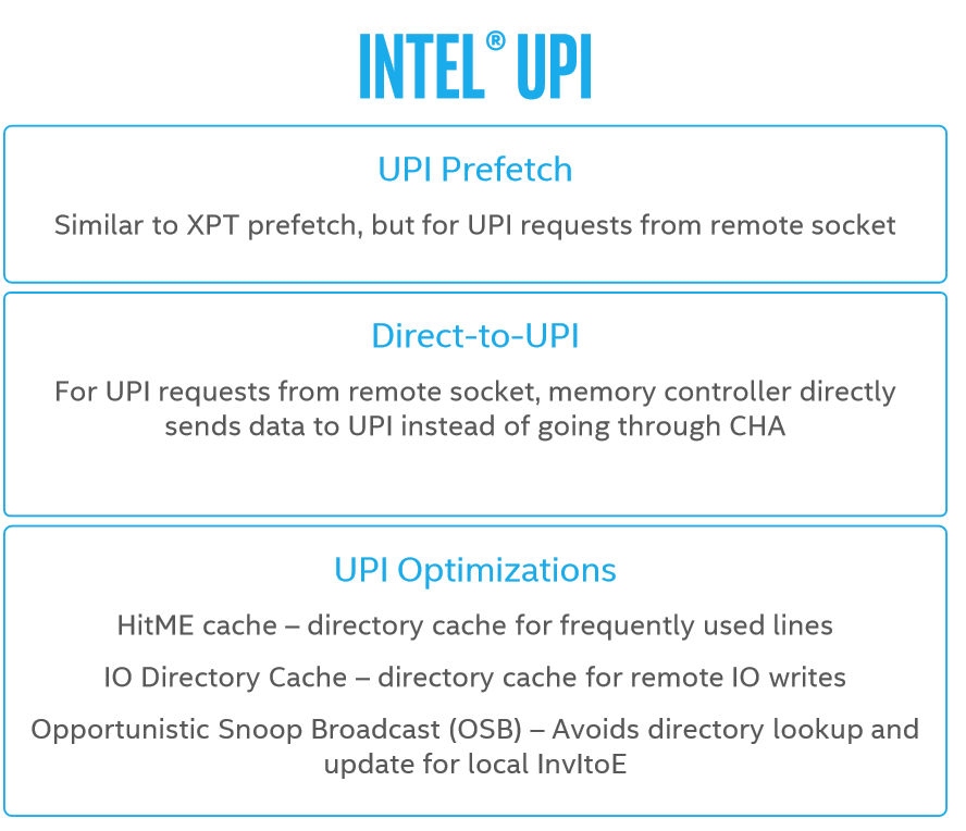
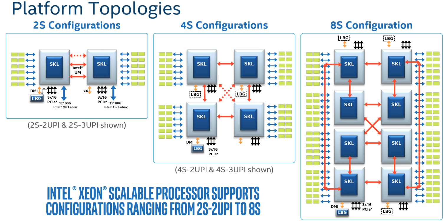
As such, Intel developed UPI to improve the data rate and power efficiency. QPI required static provisioning of resources at the target before it serviced message requests, whereas UPI has a more adaptive approach that launches requests that wait for resources to become available at the target. The distributed CHA enables for more in-flight messages to the target, which improves efficiency. A host of other improvements help enable a 4% to 21% increase in transfer efficiency per wire (at the same speed). The end result is an increase from 9.6 GT/s to 10.6 GT/s without excessive power consumption.
Increased bandwidth speeds communication, but it also has other gratuitous side effects. Much like QPI, UPI also features a L0p (low power) state that reduces throughput during periods of low activity to save power. The increased efficiency allows for even lower L0p power consumption.
MORE: Best CPUs
MORE: Intel & AMD Processor Hierarchy
MORE: All CPU Content
Current page: The Mesh Topology & UPI
Prev Page Into The Core And Cache, AVX-512 Next Page The Lewisburg Chipset
Paul Alcorn is the Editor-in-Chief for Tom's Hardware US. He also writes news and reviews on CPUs, storage, and enterprise hardware.
-
the nerd 389 Do these CPUs have the same thermal issues as the i9 series?Reply
I know these aren't going to be overclocked, but the additional CPU temps introduce a number of non-trivial engineering challenges that would result in significant reliability issues if not taken into account.
Specifically, as thermal resistance to the heatsink increases, the thermal resistance to the motherboard drops with the larger socket and more pins. This means more heat will be dumped into the motherboard's traces. That could raise the temperatures of surrounding components to a point that reliability is compromised. This is the case with the Core i9 CPUs.
See the comments here for the numbers:
http://www.tomshardware.com/forum/id-3464475/skylake-mess-explored-thermal-paste-runaway-power.html -
Snipergod87 Reply19926080 said:Do these CPUs have the same thermal issues as the i9 series?
I know these aren't going to be overclocked, but the additional CPU temps introduce a number of non-trivial engineering challenges that would result in significant reliability issues if not taken into account.
Specifically, as thermal resistance to the heatsink increases, the thermal resistance to the motherboard drops with the larger socket and more pins. This means more heat will be dumped into the motherboard's traces. That could raise the temperatures of surrounding components to a point that reliability is compromised. This is the case with the Core i9 CPUs.
See the comments here for the numbers:
http://www.tomshardware.com/forum/id-3464475/skylake-mess-explored-thermal-paste-runaway-power.html
Wouldn't be surprised if they did but also wouldn't be surprised in Intel used solder on these. Also it is important to note that server have much more airflow than your standard desktop, enabling better cooling all around, from the CPU to the VRM's. Server boards are designed for cooling as well and not aesthetics and stylish heat sink designs -
InvalidError Reply
That heat has to go from the die, through solder balls, the multi-layer CPU carrier substrate, those tiny contact fingers and finally, solder joints on the PCB. The thermal resistance from die to motherboard will still be over an order of magnitude worse than from the die to heatsink, which is less than what the VRM phases are sinking into the motherboard's power and ground planes. I wouldn't worry about it.19926080 said:the thermal resistance to the motherboard drops with the larger socket and more pins. This means more heat will be dumped into the motherboard's traces.
-
bit_user ReplyThe 28C/56T Platinum 8176 sells for no less than $8719
Actually, the big customers don't pay that much, but still... For that, it had better be made of platinum!
That's $311.39 per core!
The otherwise identical CPU jumps to a whopping $11722, if you want to equip it with up to 1.5 TB of RAM instead of only 768 GB.
Source: http://ark.intel.com/products/120508/Intel-Xeon-Platinum-8176-Processor-38_5M-Cache-2_10-GHz -
Kennyy Evony jowen3400 21 minutes agoReply
Can this run Crysis?
Jowen, did you just come up to a Ferrari and ask if it has a hitch for your grandma's trailer? -
bit_user Reply
I wouldn't trust a $8k server CPU I got for $100. I guess if they're legit pulls from upgrades, you could afford to go through a few @ that price to find one that works. Maybe they'd be so cheap because somebody already did cherry-pick the good ones.19927274 said:W8 on ebay\aliexpress for $100
Still, has anyone had any luck on such heavily-discounted server CPUs? Let's limit to Sandybridge or newer. -
JamesSneed Reply19927188 said:The 28C/56T Platinum 8176 sells for no less than $8719
Actually, the big customers don't pay that much, but still... For that, it had better be made of platinum!
That's $311.39 per core!
The otherwise identical CPU jumps to a whopping $11722, if you want to equip it with up to 1.5 TB of RAM instead of only 768 GB.
Source: http://ark.intel.com/products/120508/Intel-Xeon-Platinum-8176-Processor-38_5M-Cache-2_10-GHz
That is still dirt cheap for a high end server. An Oracle EE database license is going to be 200K+ on a server like this one. This is nothing in the grand scheme of things.
-
bit_user Reply
A lot of people don't have such high software costs. In many cases, the software is mostly home-grown and open source (or like 100%, if you're Google).19927866 said:An Oracle EE database license is going to be 200K+ on a server like this one. This is nothing in the grand scheme of things.
