Intel Xeon Platinum 8176 Scalable Processor Review
Why you can trust Tom's Hardware
Into The Core And Cache, AVX-512
The Skylake Microarchitecture
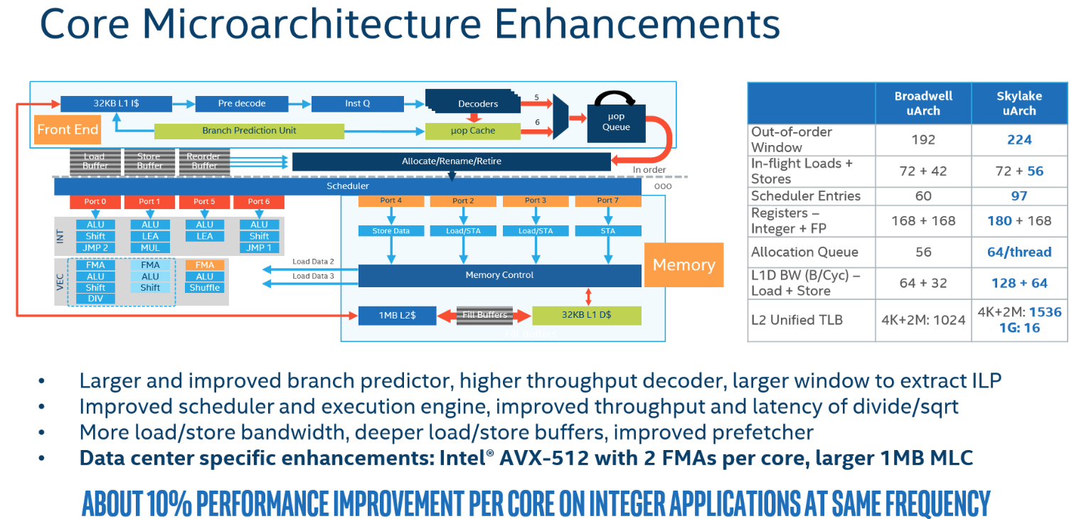
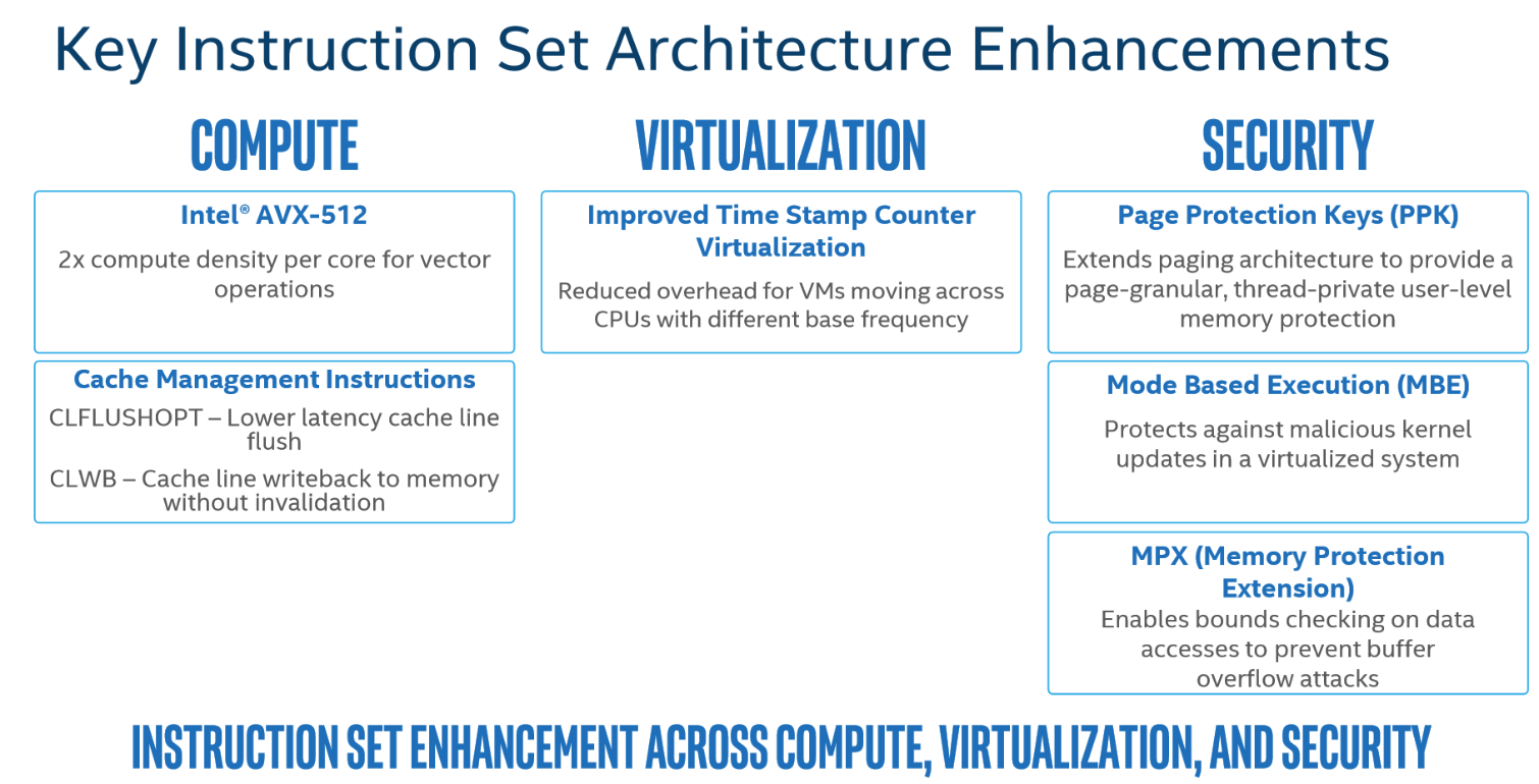
Skylake's architectural advantages over Broadwell are well-known from our desktop explorations. However, Intel added more to this particular implementation, such as AVX-512 and its re-worked cache hierarchy.
First, a quick refresher. The Skylake design first seen on mainstream desktops is fairly similar to Broadwell, which preceded it. Intel made a number of tweaks to promote instruction-level parallelism, though. Architects widened the front end and improved the execution engine with a larger re-order buffer, scheduler, integer register file, and greater retire performance. Improved decoders, branch predictor (reduced penalties for wrong jumps), and deeper load/store buffers are also among the list of enhancements. Skylake features a wider integer pipeline than its predecessor, along with a beefed-up micro-op cache (1.5x bandwidth and larger instruction window) that has an 80% hit rate.
While that was all well and good, the changes Intel makes to this revamped Skylake architecture are equally exciting.
The Skylake-SP Core - Bolt It On
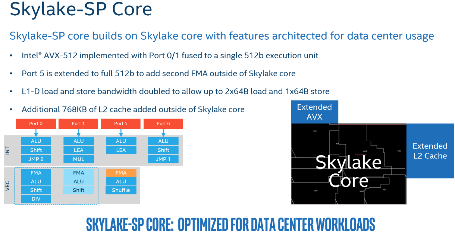
Intel enables AVX-512 by fusing port 0 and 1 into a single 512b execution unit (doubling throughput) and extending port 5 to add the second FMA unit outside of the core. That's represented as "Extended AVX" in the slide below. This facilitates up to 32 double-precision and 64 single-precision FLOPS per core.
The original core design could have supported higher L1 throughput. However, that wasn't required until Intel added the second FMA unit. Doubling the core's compute capability necessitated more throughput to prevent stalls. So, Intel doubled L1-D load and store bandwidth to keep each core fed. Now we get up to two 64-byte loads and one 64-byte store per cycle.
In addition to Skylake's 256KB per-core L2 cache, Intel tacks on 768KB more outside of the core. Our diagram isn't just a lazy mock-up. Rather, Intel specifies that the added blocks are physically outside of the original core. Data stored on the external L2 cache consequently suffers a two-cycle penalty compared to the internal L2. Still, going from 256KB to 1MB of L2 is a big deal. Greater capacity and better caching algorithms more than make up for slightly higher latency in the bigger performance picture.
Rejiggering The Cache Hierarchy
And then there's the re-architected cache hierarchy. The quadrupled L2 is still private to each core, so none of its data is shared with other cores. Each core is also associated with less shared L3 cache (from 2.5MB to 1.375MB per core).
Get Tom's Hardware's best news and in-depth reviews, straight to your inbox.
In an inclusive hierarchy, cache lines stored in L2 are duplicated in the L3. Considering the increased L2 capacity, an inclusive hierarchy would populate most of the L3 cache with duplicated data. To offset the increased L2 capacity, Intel transitioned to a non-inclusive caching scheme that doesn't require all data in the L2 to be duplicated in L3. Now the L3 serves as an overflow cache instead of the primary cache (L2 is now primary). That means only cache lines that are shared across multiple cores are duplicated in the L3 cache. The L2 cache remains 16-way associative, but the L3 drops from 20-way to 11-way.
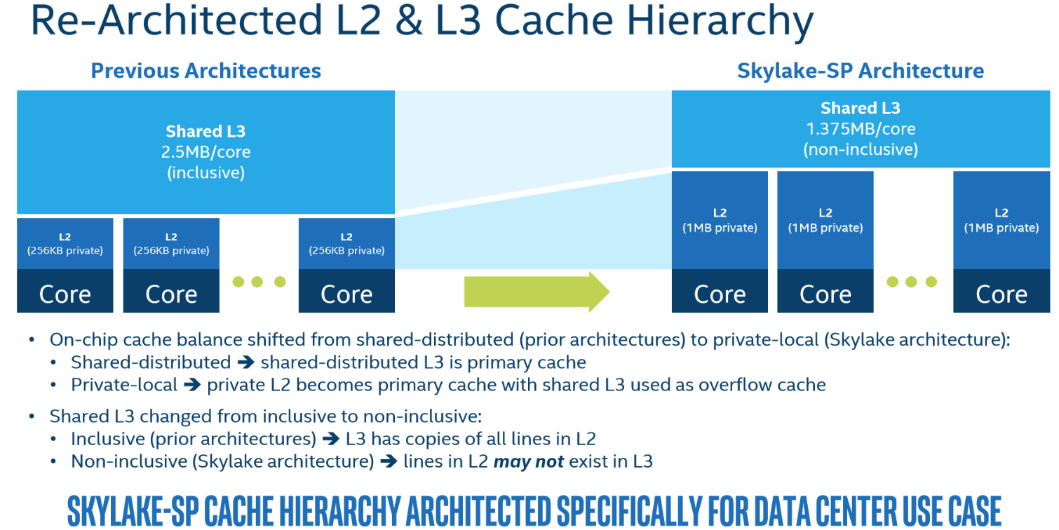
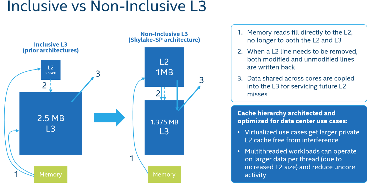
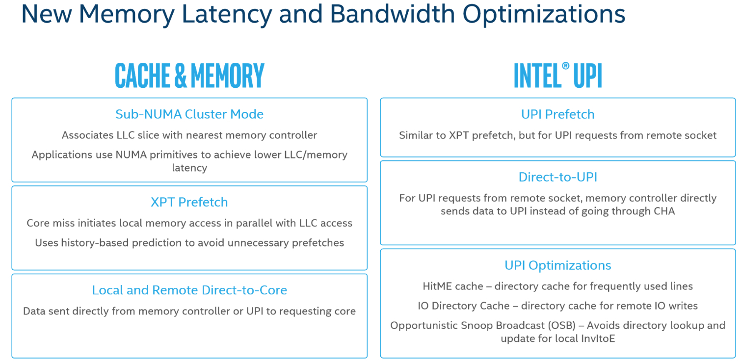
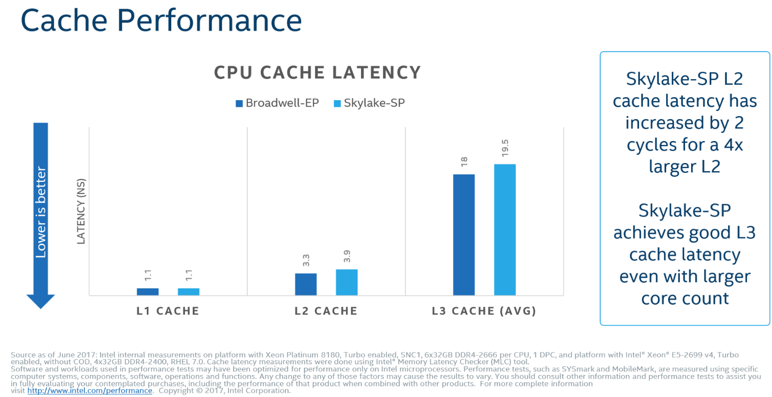
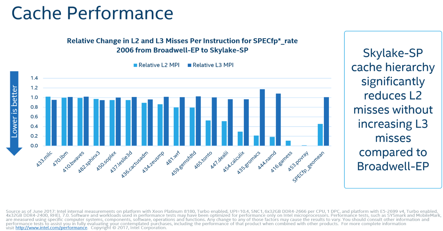
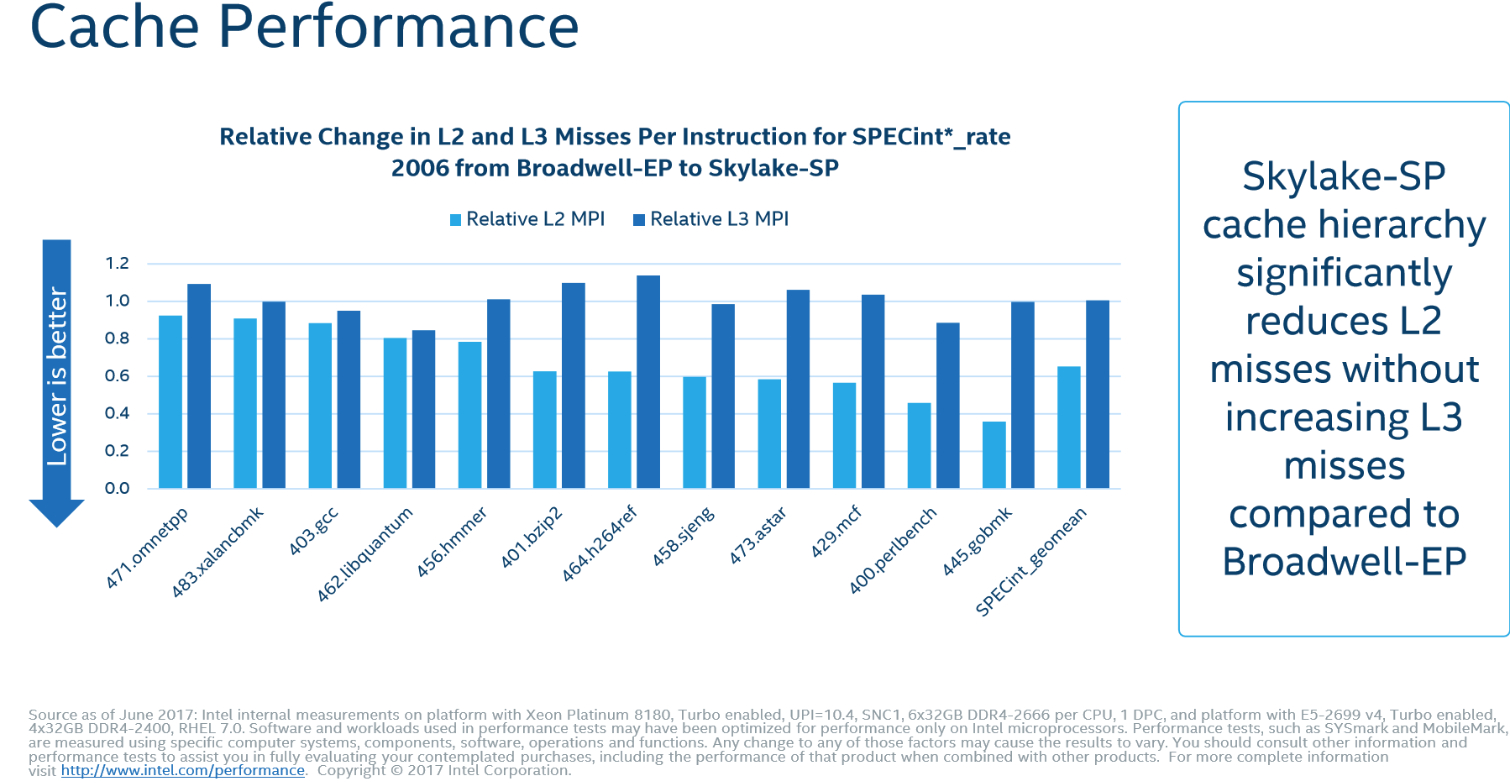
The increased L2 capacity is a boon for virtualization workloads, largely because they don't have to share the larger private L2 cache. This also grants threaded workloads access to more data per thread, reducing data movement through the mesh.
The L2 miss-per-instruction ratio is reduced in most workloads, while the L3 miss ratio purportedly remains comparable to Broadwell-EP (this varies by workload, of course). Intel provided latency benchmarks along with SPECint*_rate data to represent its L2 and L3 hit rates in common applications.
L3 latency does increase because there are more cores in the overall design. Also, the L3 cache operates at a lower frequency to match the mesh topology.
AVX-512
Intel adds AVX-512 support, which debuted with Knights Landing, to its Skylake design. However, the company doesn't support all 11 instructions. Instead, it targets specific feature sets for different market segments.
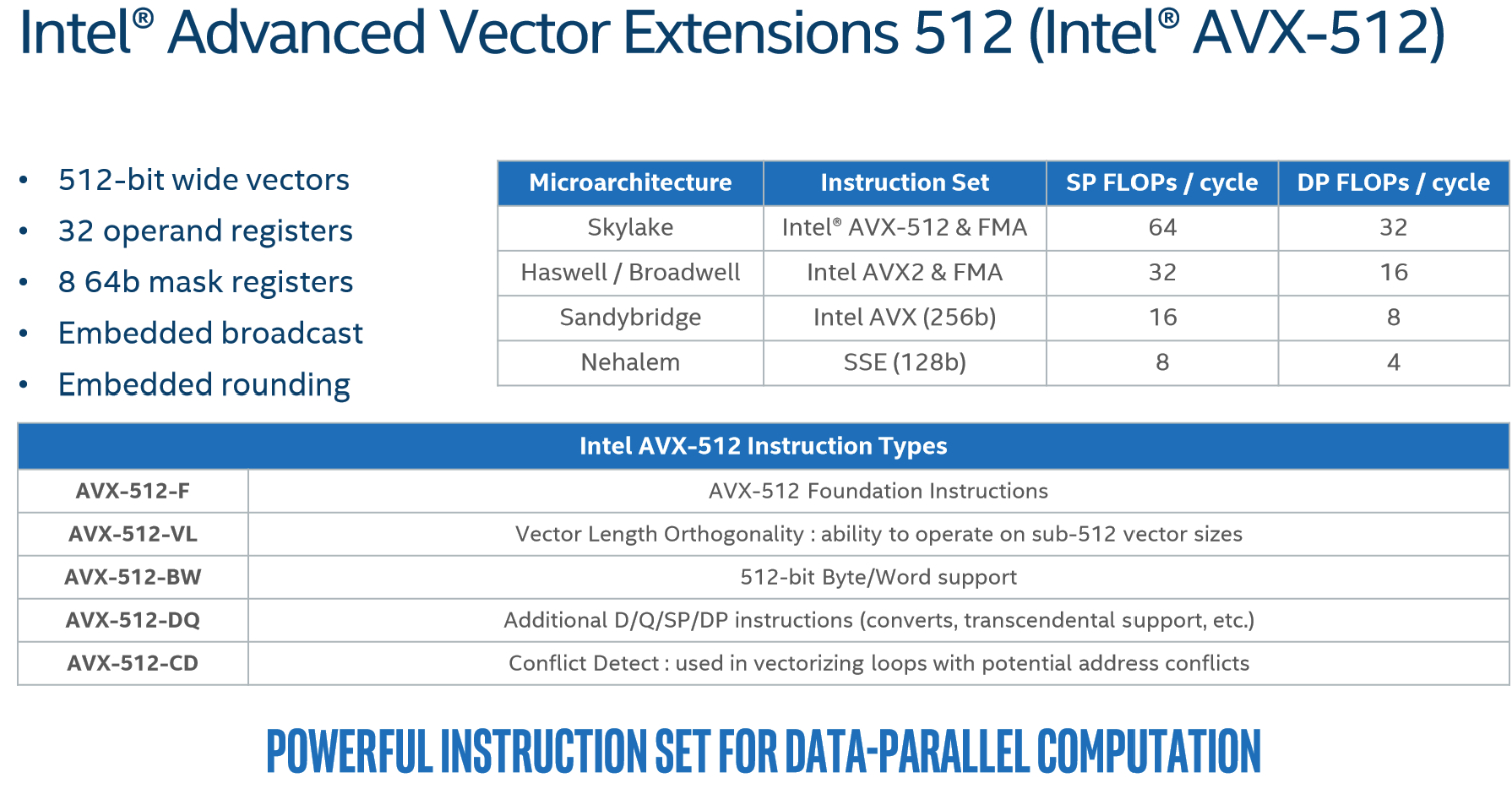
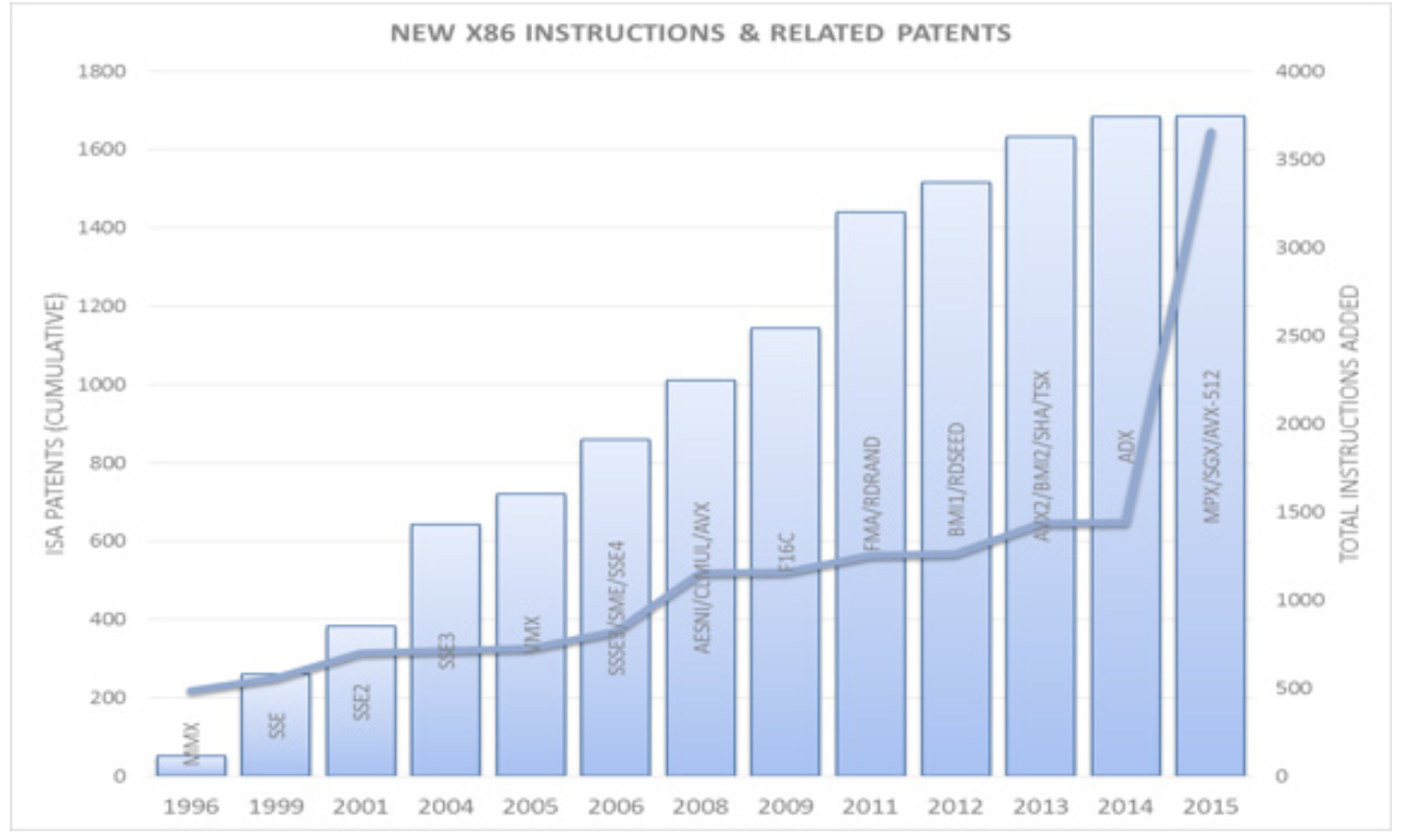
The vector unit goes from 256 bits wide to 512, the operand registers are doubled from 16 to 32, and eight mask registers are added, among other improvements. All of that returns solid gains in single- and double-precision compute performance compared to previous generations.
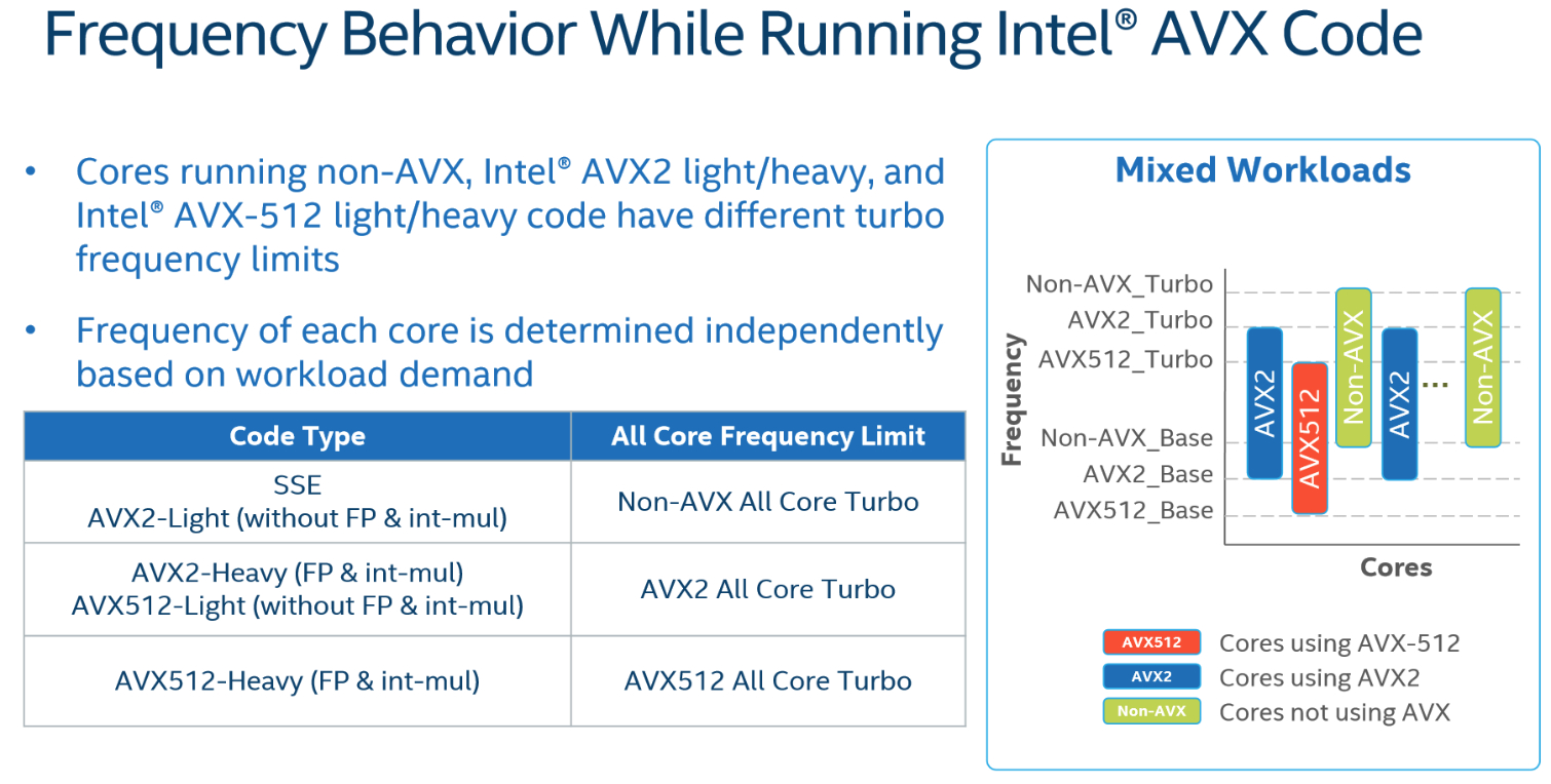
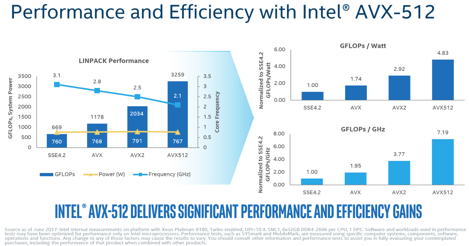
Processing AVX instructions is power-hungry work, so these CPUs operate at different clock rates based on the work they're doing. With the addition of AVX-512, there are now three sets of base and Turbo Boost frequencies (non-AVX, AVX 2.0, AVX-512), and they vary on a per-core basis. Intel's performance slide highlights that, even at lower AVX frequencies, overall compute rates increase appreciably with the instruction set. AVX-512 also dominates in both GFLOPS-per-watt and GFLOPS-per-GHz metrics.
MORE: Best CPUs
MORE: Intel & AMD Processor Hierarchy
MORE: All CPU Content
Current page: Into The Core And Cache, AVX-512
Prev Page Rebranding Xeon Next Page The Mesh Topology & UPI
Paul Alcorn is the Editor-in-Chief for Tom's Hardware US. He also writes news and reviews on CPUs, storage, and enterprise hardware.
-
the nerd 389 Do these CPUs have the same thermal issues as the i9 series?Reply
I know these aren't going to be overclocked, but the additional CPU temps introduce a number of non-trivial engineering challenges that would result in significant reliability issues if not taken into account.
Specifically, as thermal resistance to the heatsink increases, the thermal resistance to the motherboard drops with the larger socket and more pins. This means more heat will be dumped into the motherboard's traces. That could raise the temperatures of surrounding components to a point that reliability is compromised. This is the case with the Core i9 CPUs.
See the comments here for the numbers:
http://www.tomshardware.com/forum/id-3464475/skylake-mess-explored-thermal-paste-runaway-power.html -
Snipergod87 Reply19926080 said:Do these CPUs have the same thermal issues as the i9 series?
I know these aren't going to be overclocked, but the additional CPU temps introduce a number of non-trivial engineering challenges that would result in significant reliability issues if not taken into account.
Specifically, as thermal resistance to the heatsink increases, the thermal resistance to the motherboard drops with the larger socket and more pins. This means more heat will be dumped into the motherboard's traces. That could raise the temperatures of surrounding components to a point that reliability is compromised. This is the case with the Core i9 CPUs.
See the comments here for the numbers:
http://www.tomshardware.com/forum/id-3464475/skylake-mess-explored-thermal-paste-runaway-power.html
Wouldn't be surprised if they did but also wouldn't be surprised in Intel used solder on these. Also it is important to note that server have much more airflow than your standard desktop, enabling better cooling all around, from the CPU to the VRM's. Server boards are designed for cooling as well and not aesthetics and stylish heat sink designs -
InvalidError Reply
That heat has to go from the die, through solder balls, the multi-layer CPU carrier substrate, those tiny contact fingers and finally, solder joints on the PCB. The thermal resistance from die to motherboard will still be over an order of magnitude worse than from the die to heatsink, which is less than what the VRM phases are sinking into the motherboard's power and ground planes. I wouldn't worry about it.19926080 said:the thermal resistance to the motherboard drops with the larger socket and more pins. This means more heat will be dumped into the motherboard's traces.
-
bit_user ReplyThe 28C/56T Platinum 8176 sells for no less than $8719
Actually, the big customers don't pay that much, but still... For that, it had better be made of platinum!
That's $311.39 per core!
The otherwise identical CPU jumps to a whopping $11722, if you want to equip it with up to 1.5 TB of RAM instead of only 768 GB.
Source: http://ark.intel.com/products/120508/Intel-Xeon-Platinum-8176-Processor-38_5M-Cache-2_10-GHz -
Kennyy Evony jowen3400 21 minutes agoReply
Can this run Crysis?
Jowen, did you just come up to a Ferrari and ask if it has a hitch for your grandma's trailer? -
bit_user Reply
I wouldn't trust a $8k server CPU I got for $100. I guess if they're legit pulls from upgrades, you could afford to go through a few @ that price to find one that works. Maybe they'd be so cheap because somebody already did cherry-pick the good ones.19927274 said:W8 on ebay\aliexpress for $100
Still, has anyone had any luck on such heavily-discounted server CPUs? Let's limit to Sandybridge or newer. -
JamesSneed Reply19927188 said:The 28C/56T Platinum 8176 sells for no less than $8719
Actually, the big customers don't pay that much, but still... For that, it had better be made of platinum!
That's $311.39 per core!
The otherwise identical CPU jumps to a whopping $11722, if you want to equip it with up to 1.5 TB of RAM instead of only 768 GB.
Source: http://ark.intel.com/products/120508/Intel-Xeon-Platinum-8176-Processor-38_5M-Cache-2_10-GHz
That is still dirt cheap for a high end server. An Oracle EE database license is going to be 200K+ on a server like this one. This is nothing in the grand scheme of things.
-
bit_user Reply
A lot of people don't have such high software costs. In many cases, the software is mostly home-grown and open source (or like 100%, if you're Google).19927866 said:An Oracle EE database license is going to be 200K+ on a server like this one. This is nothing in the grand scheme of things.
