CL4 Or CL3: Boosts Performance By Up To 5%
When CAS Latency (latency timing) for a 200 MHz system bus (FSB) is set to CL 5.0, the column access time (tCAC) takes 50 nanoseconds and the clock cycle time (tCLK) 10 nanoseconds (this follows the well-known formula tCLK * CAS Latency >= tCAC). Other items are explained in the following table:
| RAS | Row Access Strobe |
| CAS | Column Access Strobe |
| tRCD | The time interval between RAS and CAS access |
| tRP | The time interval to switch between memory banks |
| tAC | The time interval to ready output transmission |
| tCAC | The column access time |
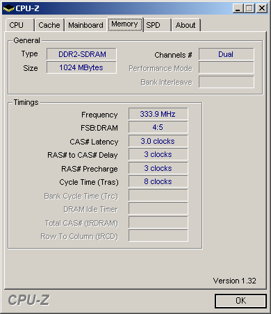
Latency information from CPU-Z on a PC running Windows XP.
A typical memory configuration looks something like this: DDR2-533 with CL 4.0 or DDR-667 with CL 5.0. Only rarely can you find DDR2 memory with nominal latency timings of CL 3.0, and when you do, it's pretty expensive because short reaction times in connection with high clock rates are difficult to achieve.

A complete set of parameters is stored in this SPD chip; the motherboard can read these directly from the memory module itself.
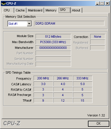
The CPU-Z program also reads SPD values directly from your memory modules.

Increasing input voltage improves signal stability.
Another concern surrounds input voltage for DDR2 memory modules. The standard level is 1.80 volts, with a tolerance of ± 0.05 volts. Some manufacturers permit their memory modules to be operated at input voltages of up to 2.2 volts. You can set input voltage levels this high for your RAM without risk, because DDR2 demands only modest power intake and thus heats up only slightly during operation. Even in our most extreme experiments we sustained no damage to our RAM modules resulting from over-voltage.
