
AMD RDNA 3 Introduction
On November 3, AMD revealed key details of its RDNA 3 GPU architecture and the Radeon RX 7900-series graphics cards. It was a public announcement that the whole world was invited to watch. Shortly after the announcement, AMD took press and analysts behind closed doors to dig a little deeper into what makes RDNA 3 tick — or is it tock? No matter.
This deep dive into the architecture primarily focuses on the RX 7900 XTX/XT (Navi 31) GPUs, though most of this applies to the Navi 32 GPUs as well. These are GPUs designed to compete with the Nvidia Ada Lovelace and RTX 40-series GPUs, to create the best graphics cards. There are other RDNA 3 details from AMD briefings, and since we originally published this RDNA 3 architectural deep dive, we've reviewed the Radeon RX 7900 XTX and 7900 XT, as well as the Radeon RX 7600.
AMD's RDNA 3 architecture fundamentally changes several of the key design elements for GPUs, thanks to the use of chiplets. And that's as good of a place to start as any. We've also got separate articles covering AMD's Gaming and ISV Relations, Software and Platform details, and the Radeon RX 7900 Series Graphics Cards.
AMD RDNA 3 Specifications
| Graphics Card | RX 7900 XTX | RX 7900 XT | RX 7800 XT | RX 7700 XT | RX 7600 |
|---|---|---|---|---|---|
| Architecture | Navi 31 | Navi 31 | Navi 32 | Navi 32 | Navi 33 |
| Process Technology | TSMC N5 + N6 | TSMC N5 + N6 | TSMC N5 + N6 | TSMC N5 + N6 | TSMC N6 |
| Transistors (Billion) | 45.6 + 6x 2.05 | 45.6 + 5x 2.05 | 28.1 + 4x 2.05 | 28.1 + 3x 2.05 | 13.3 |
| Die size (mm^2) | 300 + 225 | 300 + 225 | 200 + 150 | 200 + 113 | 204 |
| Compute Units | 96 | 84 | 60 | 54 | 32 |
| GPU Cores (Shaders) | 6144 | 5376 | 3840 | 3456 | 2048 |
| AI Cores | 192 | 168 | 120 | 108 | 64 |
| Ray Accelerators | 96 | 84 | 60 | 54 | 32 |
| Boost Clock (MHz) | 2500 | 2400 | 2430 | 2544 | 2625 |
| VRAM Speed (Gbps) | 20 | 20 | 19.5 | 18 | 18 |
| VRAM (GB) | 24 | 20 | 16 | 12 | 8 |
| VRAM Bus Width | 384 | 320 | 256 | 192 | 128 |
| Infinity Cache | 96 | 80 | 64 | 48 | 32 |
| ROPs | 192 | 192 | 96 | 96 | 64 |
| TMUs | 384 | 336 | 240 | 216 | 128 |
| TFLOPS FP32 (Boost) | 61.4 | 51.6 | 37.3 | 35.2 | 21.5 |
| TFLOPS FP16 | 122.8 | 103.2 | 75 | 70 | 43 |
| Bandwidth (GBps) | 960 | 800 | 624 | 432 | 288 |
| TBP (watts) | 355 | 315 | 263 | 245 | 165 |
| Launch Date | Dec 2022 | Dec 2022 | Sept 2023 | Sept 2023 | May 2023 |
| Launch Price | $999 | $899 | $499 | $449 | $269 |
AMD has officially launched the RX 7900 XTX/XT and RX 7600, and announced the RX 7800 XT and RX 7700 XT (coming September 6, 2023). All of the specifications and details on the 7800/7700 XT are now accurate.
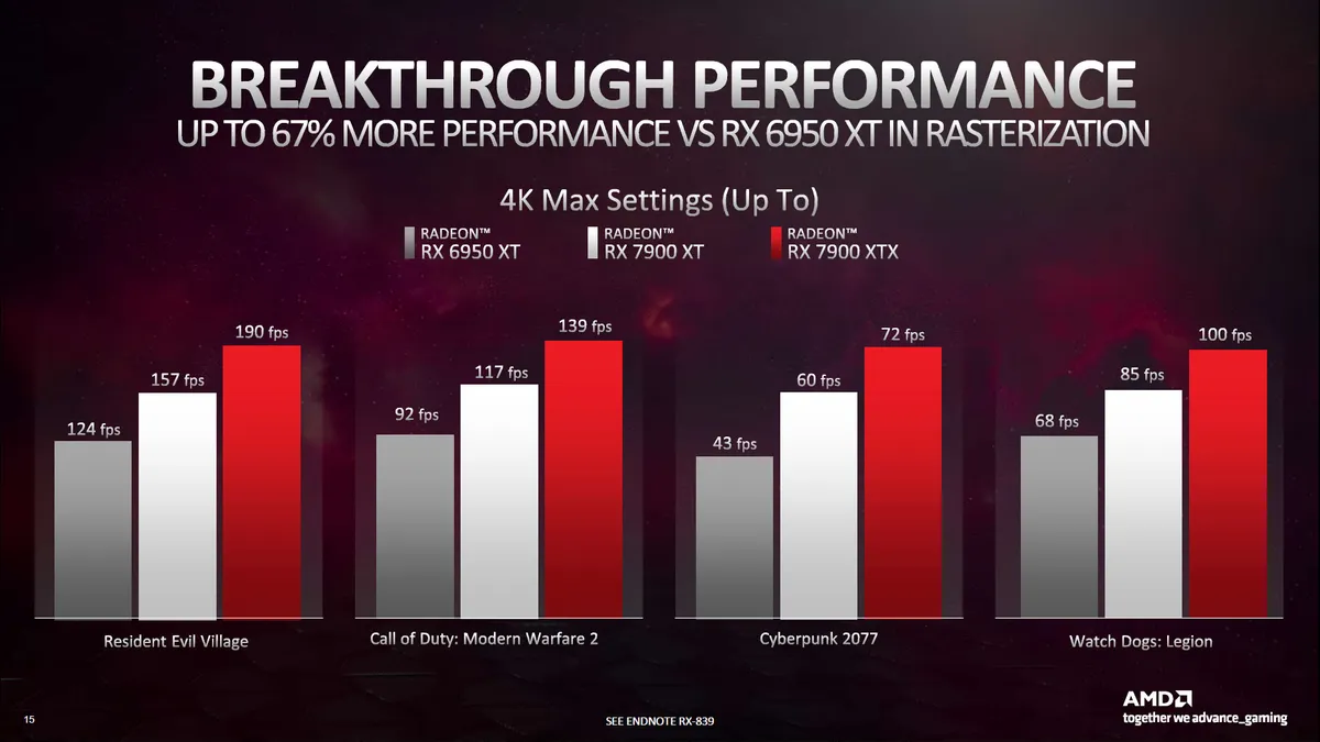
At the top, AMD provides up to 96 Compute Units (CUs) with Navi 31, but that doesn't tell the full story. The throughput for each GPU "core" has been potentially doubled relative to the previous RDNA 2 architecture. Thus, the 6144 cores on the RX 7900 XTX provide a theoretical 61.4 teraflops of FP32 performance, and double that for FP16. By way of comparison, the RX 6950 XT had 5120 cores but only 23.7 teraflops of compute.
Cache sizes are larger for the L0/L1/L2 caches, but the Infinity Cache (i.e. L3) has decreased to a maximum of 96MB on the 7900 XTX. Other GPUs include 16MB of cache per 64-bit interface.
Clock speeds have increased moderately compared to the RDNA 2 generation, depending on which GPUs you're looking at. The Navi 21 parts had official boost clocks of up to 2.31 GHz, and Navi 31 increases that to 2.5 GHz. The other Navi 2x GPUs however tended to clock in the 2.5 GHz range already, meaning the Navi 32 and 33 parts only offer incremental gains.
Pricing so far is comparable or better than the previous generation, at least in theory. In practice, once Ethereum mining ended, prices for the previous parts plummeted, with the RX 6950 XT currently selling for around $600. Likewise, the RX 7600 comes with a $269 MSRP while the previous RX 6650 XT had a $399 MSRP, but the 6650 XT has been selling for $250 or less since at least October.
Let's move on to other details of the RDNA 3 architecture.
AMD RDNA 3 and GPU Chiplets


Navi 31 consists of two core pieces, the Graphics Compute Die (GCD) and the Memory Cache Dies (MCDs). Navi 32 uses the same MCDs but has a smaller GCD. There are similarities to what AMD has done with its Zen 2/3/4 CPUs, but everything has been adapted to fit the needs of the graphics world.
For Zen 2 and later CPUs, AMD uses an Input/Output Die (IOD) that connects to system memory and provides all of the necessary functionality for things like the PCIe Express interface, USB ports, and more recently (Zen 4) graphics and video functionality. The IOD then connects to one or more Core Compute Dies (CCDs — alternatively "Core Complex Dies," depending on the day of the week) via AMD's Infinity Fabric, and the CCDs contain the CPU cores, cache, and other elements.
A key point in the design is that typical general computing algorithms — the stuff that runs on the CPU cores — will mostly fit within the various L1/L2/L3 caches. Modern CPUs up through Zen 4 only have two 64-bit memory channels for system RAM (though EPYC Genoa server processors can have up to twelve DDR5 channels).
The CCDs are small, and the IOD can range from around 125mm^2 (Ryzen 3000) to as large as 416mm^2 (EPYC xxx2 generation). Most recently, the Zen 4 Ryzen 7000-series CPUs have an IOD made using TSMC N6 that measures just 122mm^2 with one or two 70mm^2 CCDs manufactured on TSMC N5, while the EPYC xxx4 generation uses the same CCDs but with a relatively massive IOD measuring 396mm^2 (still made on TSMC N6).

GPUs have very different requirements. Large caches can help, but GPUs also really like having gobs of memory bandwidth to feed all the GPU cores. For example, even the beastly EPYC 9654 with a 12-channel DDR5 configuration 'only' delivers up to 460.8 GB/s of bandwidth. The fastest graphics cards like the RTX 4090 can easily double that.
In other words, AMD needed to do something different for GPU chiplets to work effectively. The solution ends up being almost the reverse of the CPU chiplets, with memory controllers and cache being placed on multiple smaller dies while the main compute functionality resides in the central GCD chiplet.
The GCD houses all the Compute Units (CUs) along with other core functionality like video codec hardware, display interfaces, and the PCIe connection. The Navi 31 GCD has up to 96 CUs, which is where the typical graphics processing occurs. But it also has an Infinity Fabric along the top and bottom edges (linked via some sort of bus to the rest of the chip) that then connects to the MCDs.
The MCDs, as the name implies (Memory Cache Dies) primarily contain the large L3 cache blocks (Infinity Cache), plus the physical GDDR6 memory interface. They also need to contain Infinity Fabric links to connect to the GCD, which you can see in the die shot along the center facing edge of the MCDs.
The GCD uses TSMC's N5 node and packs 45.7 billion transistors into a 300mm^2 die. The smaller Navi 32 GCD packs 28.1 billion transistors into a 200mm^2 die. The MCDs meanwhile are built on TSMC's N6 node, each packing 2.05 billion transistors on a chip that's only 37mm^2 in size. Cache and external interfaces are some of the elements of modern processors that scale the worst, and we can see that overall the GCD averages 152.3 million transistors per mm^2, while the MCDs only average 55.4 million transistors per mm^2.
It's worth mentioning here that while Navi 31 and Navi 32 use GPU chiplets, the smallest Navi 33 die (for Radeon RX 7600 and other mobile GPUs) consists of a monolithic die built on TSMC's N6 node. Cost saving measures were clearly a major factor with the various RDNA 3 designs.
AMD's High Performance Fanout Interconnect
| Interconnect | Picojoules per Bit (pJ/b) |
|---|---|
| On-die | 0.1 |
| Foveros | 0.2 |
| EMIB | 0.3 |
| UCIe | 0.25-0.5 |
| Infinity Fabric (Navi 31) | 0.4 |
| TSMC CoWoS | 0.56 |
| Bunch of Wires (BoW) | 0.5-0.7 |
| Infinity Fabric (Zen 4) | ??? |
| NVLink-C2C | 1.3 |
| Infinity Fabric (Zen 3) | 1.5 (?) |


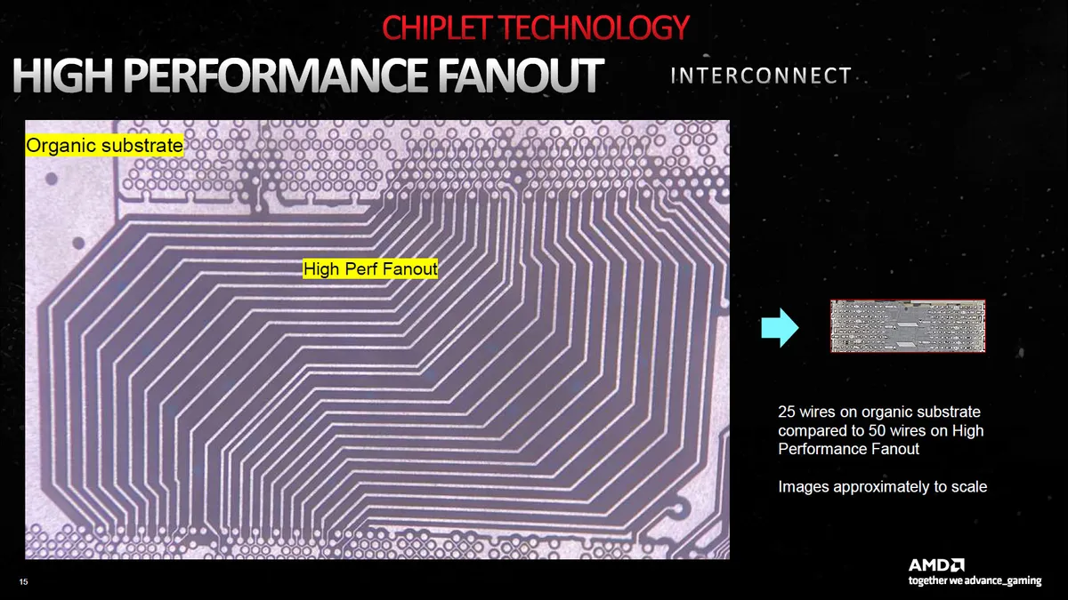

One potential concern with a chiplet approach on GPUs is how much power all of the Infinity Fabric links require — external chips almost always use more power. As an example, the Zen CPUs have an organic substrate interposer that's relatively cheap to make, but it consumes 1.5 pJ/b (Picojoules per bit). Scaling that up to a 384-bit interface would have consumed a fair amount of power, so AMD worked to refine the interface with Navi 31.
The result is what AMD calls the high performance fanout interconnect. The image above doesn't quite explain things clearly, but the larger interface on the left is the organic substrate interconnect used on Zen CPUs. To the right is the high performance fanout bridge used on Navi 31, "approximately to scale."
You can clearly see the 25 wires used for the CPUs, while the 50 wires used on the GPU equivalent are packed into a much smaller area, so you can't even see the individual wires. It's about 1/8 the height and width for the same purpose, meaning about 1/64 the total area. That, in turn, dramatically cuts power requirements, and AMD says all of the Infinity Fanout links combined deliver 3.5 TB/s of effective bandwidth while only accounting for less than 5% of the total GPU power consumption.


There's a quick interesting aside here: all the Infinity Fabric logic on both the GCD and MCDs takes up a decent amount of die space. Looking at the die shot, the six Infinity Fabric interfaces on the Navi 31 GCD use about 9% of the die area, while the interfaces are around 15% of the total die size on the MCDs.
Wipe out the Infinity Fabric interface and build the whole chip as a monolithic part on TSMC's N5 node, and it would probably only measure ~400mm^2. Apparently, the cost of TSMC N5 is so much higher than N6 that it was worth taking the chiplet route, which says something about the increasing costs of smaller fabrication nodes. It's either that or AMD is architecting for the future, taking the hit now and hoping for bigger gains later on.
Related to this, we know that certain aspects of a chip design scale better with process shrinks. External interfaces — like the GDDR6 physical interface — have almost stopped scaling. Cache also tends to scale poorly. What will be interesting to see is if AMD's next-generation GPUs (Navi 4x / RDNA 4) leverage the same MCDs as RDNA 3 while shifting the GCD to a future TSMC node like N3.
AMD RDNA 3 Architecture Upgrades

That takes care of the chiplet aspect of the design, so now let's go into the architecture changes to the various parts of the GPU. These can be broadly divided into four areas: general changes to the chip design, enhancements to the GPU shaders (Stream Processors), updates to improve ray tracing performance, and improvements to the matrix operation hardware.
Looking at the raw specs, it might not seem like AMD has increased clock speeds all that much, but previously we only had the Game Clock figures. Now we can say that the boost clocks are higher, and in general use, AMD's RDNA 3 GPUs will exceed even the official boost clocks — they're conservative boosts, in other words.
AMD says that RDNA 3 has been architected to reach speeds of 3 GHz. The official boost clocks on the reference 7900 XTX / XT are well below that mark, but we also feel AMD's reference designs focused more on maximizing efficiency. Third-party AIB cards can bump up power limits, voltages, and clock speeds quite a bit. Will we see 3 GHz out-of-factory overclocks? That didn't happen with the 7900-series, but maybe one of the other GPUs will push that far.
According to AMD, RDNA 3 GPUs can hit the same frequency as RDNA 2 GPUs while using half the power, or they can hit 1.3 times the frequency while using the same power. Ultimately, AMD wants to balance frequency and power to deliver the best overall experience. In practice, clocks on the top GPUs are a few hundred MHz higher than the previous generation.
Another point AMD makes is that it has improved silicon utilization by approximately 20%. In other words, there were functional units on RDNA 2 GPUs where parts of the chip were frequently sitting idle even when the card was under full load. Unfortunately, we don't have a good way to measure this directly, so we'll take AMD's word on this, but ultimately this should result in higher performance.
AMD RDNA 3 Compute Unit Enhancements


Outside of the chiplet stuff, many of the biggest changes occur within the Compute Units (CUs) and Workgroup Processors (WGPs). These include updates to the L0/L1/L2 cache sizes, more SIMD32 registers for FP32 and matrix workloads, and wider and faster interfaces between some elements.
AMD's Mike Mantor presented the above and the following slides, which are dense! He basically talked non-stop for the better part of an hour, trying to cover everything that's been done with the RDNA 3 architecture, and that wasn't nearly enough time. The above slide covers the big-picture overview, but let's step through some of the details.
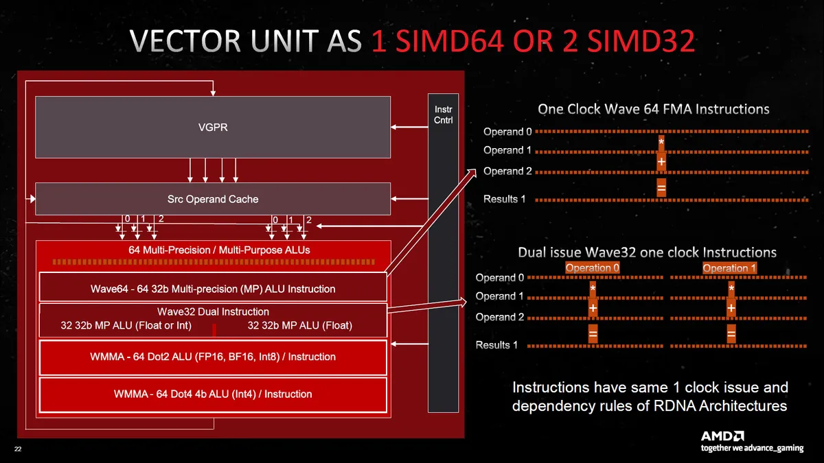
RDNA 3 comes with an enhanced Compute Unit pair — the dual CUs that became the main building block for RDNA chips. A cursory look at the above might not look that different from RDNA 2, but then notice that the first block for the scheduler and Vector GPRs (general purpose registers) says "Float / INT / Matrix SIMD32" followed by a second block that says "Float / Matrix SIMD32." That second block is new for RDNA 3, and it basically means double the floating point throughput.
You can choose to look at things in one of two ways: Either each CU now has 128 Stream Processors (SPs, or GPU shaders), and you get 12,288 total shader ALUs (Arithmetic Logic Units), or you can view it as 64 "full" SPs that just happen to have double the FP32 throughput compared to the previous generation RDNA 2 CUs.


This is sort of funny because some places are saying that Navi 31 has 6,144 shaders, and others are saying 12,288 shaders, so I specifically asked AMD's Mike Mantor — the Chief GPU Architect and the main guy behind the RDNA 3 design — whether it was 6,144 or 12,288. He pulled out a calculator, punched in some numbers, and said, "Yeah, it should be 12,288." And yet, in some ways, it's not.
AMD's own specifications say 6,144 SPs and 96 CUs for the 7900 XTX, and 84 CUs with 5,376 SPs for the 7900 XT, so AMD is taking the approach of using the lower number. However, raw FP32 compute (and matrix compute) has doubled. Personally, it makes more sense to me to call it 128 SPs per CU rather than 64, and the overall design looks similar to Nvidia's Ampere and Ada Lovelace architectures. Those now have 128 FP32 CUDA cores per Streaming Multiprocessor (SM), but also 64 INT32 units. But whatever the case, AMD isn't using the larger numbers.
Along with the extra 32-bit floating-point compute, AMD also doubled the matrix (AI) throughput, and the AI Matrix Accelerators share many of the shader execution resources. New to the AI units is BF16 (brain-float 16-bit) support, as well as INT4 WMMA Dot4 instructions (Wave Matrix Multiply Accumulate), and as with the FP32 throughput, there's an overall 2.7x increase in matrix operation speed.
That 2.7x appears to come from the overall 17.4% increase in clock-for-clock performance, plus 20% more CUs and double the SIM32 units per CU. (But don't quote me on that, as AMD didn't specifically break down all of the gains.)
AMD RDNA 3: Bigger and Faster Caches and Interconnects

The caches, and the interfaces between the caches and the rest of the system, have all received upgrades. For example, the L0 cache is now 32KB (double RDNA 2), and the L1 caches are 256KB (double RDNA 2 again), while the L2 cache increased to 6MB (1.5x larger than RDNA 2).
The link between the main processing units and the L1 cache is now 1.5x wider, with 6144 bytes per clock throughput. Likewise, the link between the L1 and L2 cache is also 1.5x wider (3072 bytes per clock).
The L3 cache, also called the Infinity Cache, did shrink relative to Navi 21. It's now 96MB vs. 128MB. However, the L3 to L2 link is now 2.25x wider (2304 bytes per clock), so the total throughput is much higher. In fact, AMD gives a figure of 5.3 TB/s — 2304 B/clk at a speed of 2.3 GHz. The RX 6950 XT only had a 1024 B/clk link to its Infinity Cache (maximum), and RDNA 3 delivers up to 2.7x the peak interface bandwidth.
Note that these figures are only for the fully configured Navi 31 solution in the 7900 XTX. The 7900 XT has five MCDs, dropping down to a 320-bit GDDR6 interface and 1920 B/clk links to the combined 80MB of Infinity Cache. We will see lower-tier RDNA 3 parts that further cut back on interface width and performance, naturally.
Finally, there are now up to six 64-bit GDDR6 interfaces for a combined 384-bit link to the GDDR6 memory. The VRAM also clocks at 20 Gbps (vs 18 Gbps on the later 6x50 cards and 16 Gbps on the original RDNA 2 chips) for a total bandwidth of 960 GB/s.
It's interesting how much the gap between GDDR6 and GDDR6X has narrowed with this generation, at least for shipping configurations. AMD's 960 GB/s on the RX 7900 XTX is only 5% less than the 1008 GB/s of the RTX 4090 now, whereas with the RX 6900 XT and RTX 3090 were only pushing 512 GB/s compared to Nvidia's 936 GB/s back in 2020. Nvidia of course also adopted a larger cache size with its Ada Lovelace architecture.
AMD RDNA 3: 2nd Generation Ray Tracing
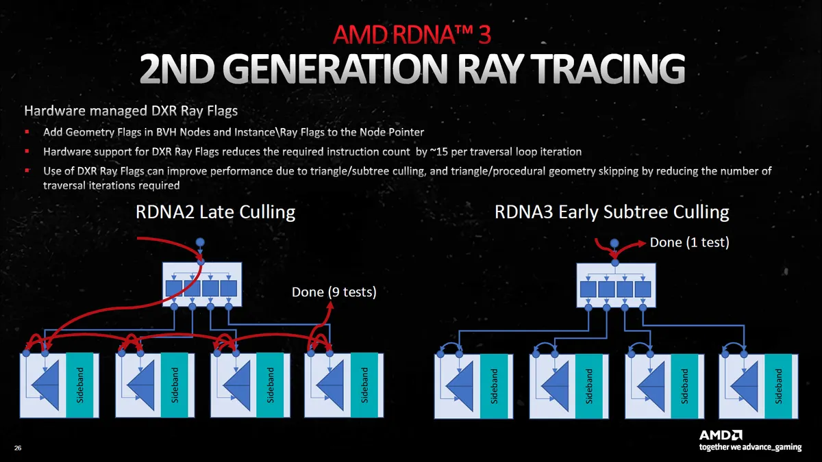
Ray tracing on the RDNA 2 architecture always felt like an afterthought — something tacked on to meet the required feature checklist for DirectX 12 Ultimate. AMD's RDNA 2 GPUs lack dedicated BVH traversal hardware, opting to do that work via other shared units, and that's at least partially to blame for their weaker RT performance.
RDNA 2 Ray Accelerators could do up to four ray/box intersections per clock, or one ray/triangle intersection. By way of contrast, Intel's Arc Alchemist can do up to 12 ray/box intersections per RTU per clock, while Nvidia doesn't provide a specific number but has up to two ray/triangle intersections per RT core on Ampere and up to four ray/triangle intersections per clock on Ada Lovelace.
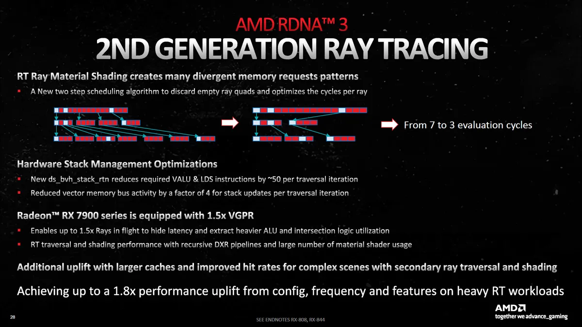
It's not clear if RDNA 3 actually improves those figures directly or if AMD has focused on other enhancements to reduce the number of ray/box intersections performed. Perhaps both. What we do know is that RDNA 3 will have improved BVH (Bounding Volume Hierarchy) traversal that will increase ray tracing performance.
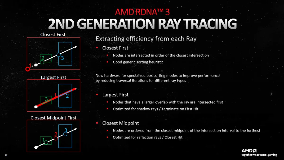
RDNA 3 also has 1.5x larger VGPRs (Vector General Purpose Registers), which means 1.5x as many rays in flight. There are other stack optimizations to reduce the number of instructions needed for BVH traversal, and specialized box sorting algorithms (closest first, largest first, closest midpoint) can be used to extract improved efficiency.
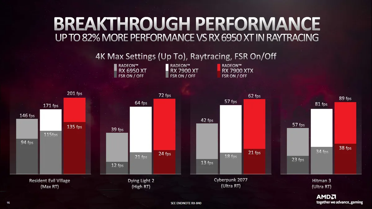
Overall, thanks to the new features, higher frequency, and increased number of Ray Accelerators, AMD says RDNA 3 should deliver up to a 1.8x performance uplift for ray tracing compared to RDNA 2. That should narrow the gap between AMD and Nvidia Ampere. Still, Nvidia also seems to have doubled down on its ray tracing hardware for Ada Lovelace, so we wouldn't count on AMD delivering equivalent performance to RTX 40-series GPUs. (You can see the current results in our GPU benchmarks hierarchy.)
AMD RDNA 3: Other Architectural Improvements

Finally, RDNA 3 has tuned other elements of the architecture related to the command processor, geometry, and pixel pipelines. There's also a new Dual Media Engine with support for AV1 encode/decode, AI-enhanced video decoding, and the new Radiance Display Engine.
The Command Processor (CP) updates should improve performance for certain workloads while also reducing CPU bottlenecks on the driver and API side. Hardware-based culling performance is also 50% faster on the geometry side of things, and there's a 50% increase in peak rasterized pixels per clock.
That last seems to be a result of increasing the number of ROPs (Render Outputs) from 128 on Navi 21 result to 192 on Navi 31. That makes sense, as there's also a 50% increase in memory channels, and AMD would want to scale other elements in step with that.
The Dual Media Engine should bring AMD up to parity with Nvidia and Intel on the video side of things, though our most recent video codec quality and performance testing shows it still lags behind Intel and Nvidia. Also note that AV1 is more about getting rid of HEVC's royalty fees rather than improving quality, though performance can be a bit of a wild card.
AMD also gains at least a few points for including DisplayPort 2.1 support. Intel also has DP2 support on its Arc GPUs, but it tops out at 40 Gbps (UHBR 10), while AMD can do 54 Gbps (UHBR 13.5). AMD's display outputs can drive up to 4K at 229 Hz without compression for 8-bit color depths, or 187 Hz with 10-bit color. Display Stream Compression can more than double that, allowing for 4K and 480 Hz or 8K and 165 Hz — not that we're anywhere near having displays that actually support such speeds.
Realistically, we have to wonder how important DP2.1 UHBR 13.5 will be with the RDNA 3 graphics cards. You'll need a new monitor that supports DP2.1 first of all, and second, there's the question of how much better something like 4K 180 Hz looks with and without DSC — because DP1.4a can still handle that resolution with DSC while UHBR 13.5 could do it without DSC. We've been using a Samsung Odyssey Neo G8 32-inch display with 4K 240 Hz support, via DSC, and couldn't spot any degradation in quality.
AMD RDNA 3: Closing Thoughts


For those who want the full collection of slides on the RDNA 3 architecture, you can flip through them in the above gallery. Overall, it sounds like an impressive feat of engineering. You can also check our Radeon RX 7900 XTX/XT review to see how the RDNA 3 GPUs stack up.
AMD can compete quite well against Nvidia's RTX 4080 card, at least for non ray tracing and non-AI workloads. On the other hand, if you want the fastest GPU around, AMD doesn't even attempt to go head-to-head against the bigger RTX 4090.
Simple math provides plenty of food for thought. With FP32 6,144 shaders running at 2.5 GHz with double the ALU throughput, versus Nvidia's 16,384 shaders at 2.52 GHz, Nvidia clearly has the raw compute advantage — 61 teraflops vs. 83 teraflops. As noted, adding more FP32 units makes AMD's RDNA 3 seem more like Ampere and Ada Lovelace.
Beyond raw compute, we've got transistor counts and die sizes. Nvidia is sticking with monolithic dies for Ada Lovelace, with AD102, AD103, AD104, AD106, and AD107 chips. The largest has 76.3 billion transistors in a 608mm^2 chip. Even if AMD were doing a monolithic 522mm^2 chip with 58 billion transistors, we'd expect Nvidia to have some advantages. However, the GPU chiplet approach means some of the area and transistors get used on things not directly related to performance.
Meanwhile, Nvidia's penultimate Ada chip, the AD103 used in the RTX 4080, falls on the other side of the fence. With a 256-bit interface, 45.9 billion transistors, and a 368.6mm^2 die size, Navi 31 should have some clear advantages — both with the RX 7900 XTX and the slightly lower tier 7900 XT. And then there's AD104 with 35.8 billion transistors and a 294.5mm^2 die, the "unlaunched" RTX 4080 12GB that eventually morphed into the RTX 4070 Ti.
But there's more to performance than paper specs. Nvidia invests transistors into features like DLSS (Tensor cores), DLSS 3 (the Optical Flow Accelerator), and ray tracing hardware. AMD seems more willing to give up some ray tracing performance while boosting the more common use cases. In practice, the RX 7900 XTX barely leads the RTX 4080 in rasterization performance in our GPU benchmarks hierarchy, while in ray tracing performance it's more of a match for the previous generation RTX 3090.
For those who aren't interested in graphics cards costing $900 or more, there are also cards like the RTX 4070 Ti, RTX 4070, RTX 4060 Ti, and RX 7600. We're still waiting for AMD's RX 7800 and 7700 offerings, which are likely delayed while AMD waits to clear out remaining Navi 2x inventory. Navi 32 is rumored to use the same MCDs, but with a smaller GCD, while Navi 33 has already launched as a monolithic die still built on the N6 node.
Note: This article has been updated since it was originally published to include additional details now that the RDNA 3 GPUs are available.
- MORE: Best Graphics Cards
- MORE: GPU Benchmarks and Hierarchy
- MORE: All Graphics Content
