Antec Aria AR300 PSU Repair
Have you ever bought a computer case with a proprietary PSU form factor? What do you do when it eventually wears out? One option is to repair it.
Revisiting The Photocoupler
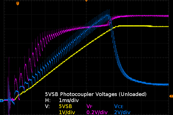
Remember those noisy-looking feedback photocoupler output waveforms I did not like earlier? Now that I have something that seems like a definitive fix, I decided to go back and have another look:


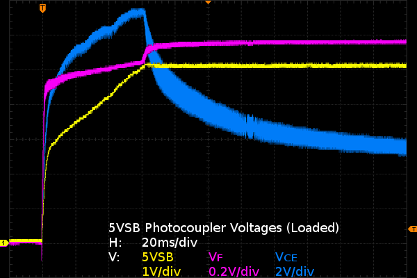
And sure enough, these look a lot more like what I was originally expecting. Here, VF is the voltage across the photocoupler's LED on the secondary side, while VCE is the voltage across the photocoupler's collector-emitter terminals on the primary side. As with previous photocoupler waveforms, nothing exciting happens before the 5VSB voltage actually reaches 5V. Until then, VF simply follows the TL431's minimum operating current. The VCE ramp merely follows the 5VSB and AUX2 voltage ramps since it is open-circuit. What changed is that we have no more negative spiking and no more 10-15V peak-to-peak noise on VCE, only a relatively smooth control signal with the error output from the 5VSB's TL431 coupled through the 817 on top. Putting some load on the 5VSB rail causes the TL431 to draw less current through the photodiode to maintain its reference voltage, which in turn reduces the phototransistor's current and allows VCE to increase, reducing the 5VSB transformer's triggering rate and power output.
On the unloaded waveform, you may have noticed how the pulse rate increases as the output voltage ramps up. The reason is that it takes longer for inductors to dump energy into low-impedance loads like discharged capacitors. You've probably heard the classic xenon flash capacitor bank charging noise: a low coil whine that ramps up to ultrasonic pitch over a few seconds. It is caused by the exact same principle.
Get Tom's Hardware's best news and in-depth reviews, straight to your inbox.
Current page: Revisiting The Photocoupler
Prev Page Do We Have A Fix? Next Page More Complementary Curiosity-
iam2thecrowe That was a good read. I have a lot of custom power supplies (not PC atx) that i would like to fix at work instead of replace, would be a lot cheaper (there's some high wattage power supplies that cost $5000 to replace). Need to convince the boss to buy a good oscilloscope.Reply -
Rookie_MIB I have several of those cases - they make nice little machines for office use but the PSUs tend to flake. I've had to replace several...Reply -
Daniel Sauvageau All the standby power supplies I remember looking at are of the good old flyback design and one particularity of the flyback topology is that it has the worst ripple current on the output capacitors of all converter topologies or in other words: it is the harshest on output capacitors. Until I saw the waveforms while poking around the SL300, one little yet important detail skipped my mind: the harsh current waveform behavior applies to ALL outputs.Reply
Any flyback supply with sub-par output capacitors on any of its outputs will inevitably fail in relatively short order.
After that 'oops' moment, I decided to pop the lid on my LG 204WT which I thought had dying CCFL tubes, popped three of its auxiliary supply capacitors off the board, measured them at 5-20 ohms of ESR, replaced them, no more flicker or random turn-on issues. -
gnyff I love it when stuff is repaired! It's so sad that almost every consumer device today is made to fail and be replaced. Even in the cases where the designer did not specifically design for failure most commonly it's definitely not cost-effective for the user to have it repaired. :-(Reply
Anyways, I've also replaced one of those lousy non-standard PSU. Hard to find and depressingly expensive. Thus, I am avoiding non-standard parts as much as possible now! ;-)
By the way, in one of my systems the standby power was around 12W (!) even after shutting off 5VSB functions (wake on LAN, keyboard etc) in the BIOS. I did on bother to investigate further (thinking "lousy supply"!) and simply added a proper "full off" power switch. Probably other owners should think of doing the same ;-) -
Rookie_MIB Reply16509494 said:Anyways, I've also replaced one of those lousy non-standard PSU. Hard to find and depressingly expensive. Thus, I am avoiding non-standard parts as much as possible now! ;-)
By the way, in one of my systems the standby power was around 12W (!) even after shutting off 5VSB functions (wake on LAN, keyboard etc) in the BIOS. I did on bother to investigate further (thinking "lousy supply"!) and simply added a proper "full off" power switch. Probably other owners should think of doing the same ;-)
I wonder if a SFX PSU could be mounted in those cases. Might be a viable solution... -
nukemaster Another great one!Reply
I actually was interested in that case back when it was released, but just kept rocking the Sonata and Sonata II. While my power supplies did not fail. caps leaked after a while(power supplies still worked)and I took the power supplies out of service forever.
Rookie_MIB,
SFX would be an interesting idea to see for sure. My SFX is still going after 5 years of 24/7 operation(not bad for a case included 300 watt unit). -
Daniel Sauvageau Reply
The dimensions might fit but mounting holes would be on the wrong side (for mounting in a way that might fit internally) and the IEC socket would face either the motherboard or the top cover. Nothing some drill-and-tapping with some wire splicing cannot fix for people who would favor this route instead of a repair of the existing unit where that is possible.16509868 said:I wonder if a SFX PSU could be mounted in those cases. Might be a viable solution...
BTW, the total repair cost for the 5VSB side is about $1.50 for the caps and resistor. The rest is basically free since I scavenged the SCs from a dead (catastrophic primary-side failure) PSU and would have cost around $2.50 otherwise. If Asus had specified higher quality parts from Channel Well though, the PSU may have cost less than $0.50 extra to get right on the first try. Evem doing as little as specifying Teapo SC as the minimum requirement would have easily doubled the trouble-free service life over using SEK..
It always bugs me when only a few pennies worth in parts and materials can spell the difference between a product that might only last 2-3 years and a product that should easily last 10+ years. -
nukemaster That small cost per unit adds up.Reply
I can not count the number of times I say, gee a xx cent part would have solved this damn issue and yet no one does it.
Drilling and making it fit is no issue. :)
I still get my small system fix with an SG05 case.
Where do you get your parts from? Digikey is not too expensive, but many times the shipping cost more than the parts(especially with resistors that are cheap to begin with.). -
Daniel Sauvageau Reply
The "small cost" may add up but if you charge $1 to put the $0.50 worth of better quality parts in, you still make a 100% profit on that extra cost and you score points in the quality/reliability column. For the most part, those better quality parts are the same physical size, so no fitting or PCB layout concerns there.16511613 said:That small cost per unit adds up.
Where do you get your parts from? Digikey is not too expensive, but many times the shipping cost more than the parts(especially with resistors that are cheap to begin with.).
As for where I get my parts, they are mostly Digikey. I either lump my order with parts I need to repair something for someone else (and pass the shipping cost to them) or build my order for multiple non-urgent projects until it qualifies for free shipping.
Edit: and for things like 0805 resistors and capacitors, I usually order in cut-tapes of 100 since we're still only talking $1-2 there. If I had more storage space, I would order whole reels for $10-15 (2000-3000 units) and likely never have to worry about ordering more of that resistor or capacitor value (for personal use) for the rest of my life. -
pjmelect I often repair computer power supplies and I enjoyed reading this article. One comment, that may help others and may explain some things in the article such as the power reduction of the fixed power supply.Reply
Capacitors with high ESR always have a very high leakage current near their rated voltage. The leakage current at low multi-meter voltage levels is not normally measurable, but increasing the voltage across the capacitor dramatically increases the leakage. Circuits with capacitors with high ESR in them normally fail not due to the ESR or the reduction of capacitance, but due to the high leakage current. If you do not have a ESR meter you can simply put a suspect capacitor across a power supply at its rated voltage and check the leakage current. A high leakage current is a good indication of a high ESR value.
I use a in-circuit ESR meter to test all of the electrolytic capacitors (even the small ones) before I even start trying to fault find a power supply.