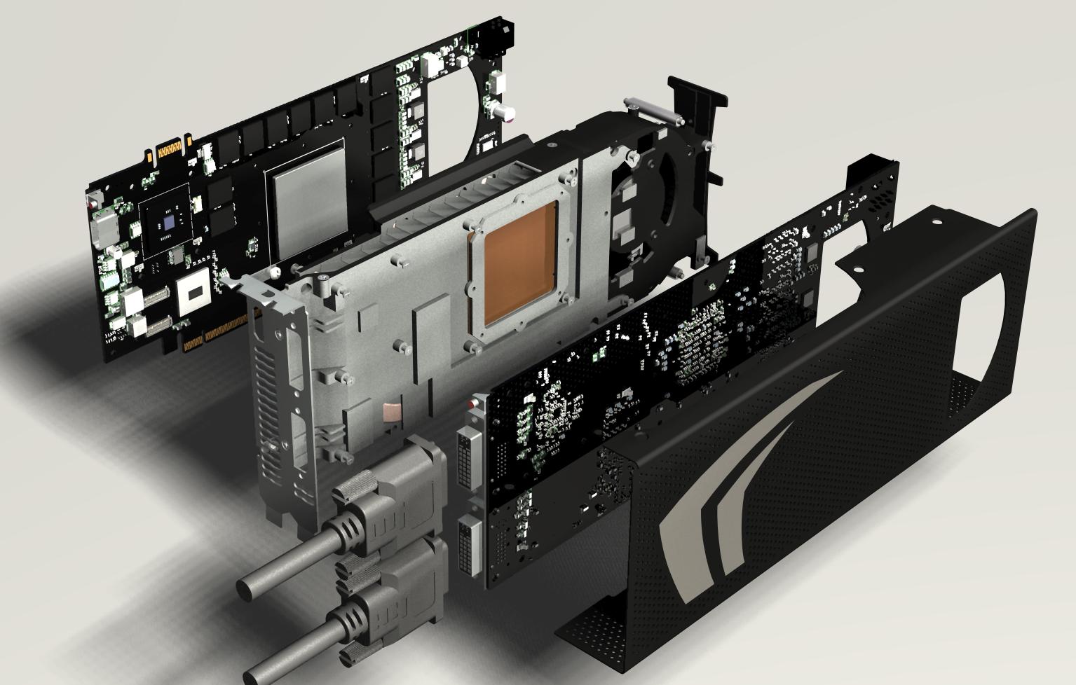
GeForce GTX 295 In Quad-SLI

Get Tom's Hardware's best news and in-depth reviews, straight to your inbox.
You are now subscribed
Your newsletter sign-up was successful
Meet The New "GX2"
Rumors of a GT200-based dual-GPU solution from Nvidia quickly began circulating after AMD’s Radeon HD 4870 X2 knocked the GeForce GTX 280 from its performance throne. Nvidia certainly had the design experience, with its GeForce 7950 GX2 and GeForce 9800 GX2 paving the way for further improvements in its multiple-GPU product line. However, those rumors were quickly quashed by the logic that two full GTX 280 processors at 65nm would require too much power and create too much heat to be combined in a single package.
A recent die-process shrink from 65nm to 55nm helped to reduce both heat and power consumption, allowing Nvidia to pursue its two-cards-in-a-brick GX2 design using the most recent variation of its high-end graphics processor. As with previous GX2 products, Nvidia further reduced heat and power consumption by slightly downgrading its twin graphics processors. The new board uses the memory interface and clock speeds of its GeForceGTX 260, but with the full 240 stream processors its GeForce GTX 280 is known for.
Given Nvidia’s propensity for recycling the names of former high-end parts, one might have expected the company to call its new product the “GTX 280 GX2” or “GTX 380 GX2”. Instead, it chose a middle road, removing the GX2 designation to title this product the GeForce GTX 295.
We saw excellent performance in our GeForce GTX 295 preview, but wondered what advancements improved drivers could bring. Also in the backs of our minds were SLI scaling issues that had plagued 7950 GX2 and 9800 GX2 Quad-SLI configurations, causing these to fall behind SLI pairs of single-GPU 7900 GTX and 8800 GTX cards at ultra-high graphics settings. With these questions in mind, we set about procuring a second GTX 295 unit and two HD 4870 X2 cards for comparing Quad SLI to CrossFireX performance, plus three GTX 280 cards to compare Nvidia’s highest-end 3-way SLI to its current Quad-SLI solution.
Get Tom's Hardware's best news and in-depth reviews, straight to your inbox.
-
JeanLuc I’m looking at page 9 on the power usage charts – I have to say the GTX295 is very impressive it’s power consumption isn’t that much greater then the GTX280. And what’s very impressive is it uses 40% less power in SLI then the HD4870X2 does in Crossfire., meaning if I already owned a pretty decent PSU say around 700-800 watt’s I wouldn’t have to worry about getting it replaced if I were planning on SLIing the GTX295.Reply
I would have liked to have seen some temperatures in there somewhere as well. With top end cards becoming hotter and hotter (at least with ATI) I wonder if cheaper cases are able to cope with the temperatures these components generate.
BTW any chance of doing some sextuple SLI GTX295 on the old Intel Skulltrail?
-
Crashman JeanLucBTW any chance of doing some sextuple SLI GTX295 on the old Intel Skulltrail?Reply
Not a chance: The GTX 295 only has one SLI bridge connector. NVIDIA designs its products intentionally to only support a maximum of four graphics cores, and in doing so eliminates the need to make its drivers support more. -
neiroatopelcc I'd like to see a board that takes up 3 slots, and use both the 1st and the 3rd slot's pcie connectors to power 4 gpu's on one board. Perhaps with the second pcie being optional - so in case of not fitting the card at all, one could fit it with reduced bandwidth. That way they'd have a basis to make some proper cooling. Perhaps a small h2o system, or a peltier coupled with some propler fan and heatsink.Reply
ie. a big 3x3x9" box resting on the expansion slots, dumping warm air outside. -
jameskangster "...Radeon HD 4870 X2 knocked the GeForce GTX 280 from its performanceReply
thrown." --> "throne"? or am I just misunderstanding the sentence? -
kschoche So the conclusion should read:Reply
Congrats on quad-sli, though, for anything that doesnt already get 100+ fps with a single GX2, you're welcome to throw in a second and get at most a 10-20% increase, unless of course you want to get an increase to a game that doesnt already have 100 FPS (crysis), in which case you're screwed - dont even bother with it. -
duzcizgi Why test with AA and AF turned on with such high end cards? Anyone who pays +$400 * X wouldn't be playing any game with AA AF turned off or with low res. display. (If I'd pay $800 for graphics cards, I'd have of course had a display with no less than 1920x1200 resolution. Not even 1680x1050)Reply
And I'm a little disappointed with the scaling of all solutions. They still don't scale well. -
hyteck9 The performance per watt char is exactly what I wanted to see (it would be even better with some temps listed though). Thanks THG, This will help things along nicely.Reply -
duzcizgi, don't forget about the real hardcore players (those who play tournaments for example), who prefer to play with the lower graphics settings and ensure > 100 FPS.Reply

