Radeon HD 6970 And 6950 Review: Is Cayman A Gator Or A Crock?
Last month, Nvidia launched its GeForce GTX 580, but we told you to hold off on buying it. A week ago, Nvidia launched GeForce GTX 570 and we again said "wait." AMD's Cayman was our impetus. Were Radeon HD 6970 and 6950 worth the wait? Read on for more!
Building Cayman By Improving Cypress
According to AMD, it had four principal design goals in building Cayman: more efficiency, improved geometry performance, new image quality features, and better power management.
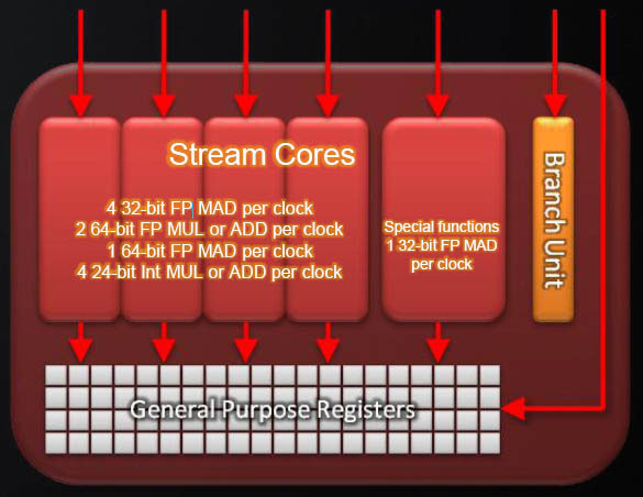
First, it wanted to create a more efficient graphics and compute architecture. The motivation behind this decision is sound enough—AMD was seeing a VLIW rate of roughly 3.4 in games. So, removing the special function transcendental unit and distributing its functionality across the other four units was actually a good performance per area optimization that promised to keep the GPU running within the observed operating rate. There are situations where performance could take a hit (when the VLIW utilization spikes above four), but AMD says that's unlikely.
More important, AMD needed to create a more efficient architecture. Stuck on TSMC’s 40 nm manufacturing node, the company had to figure how to get more performance per millimeter of die space, rather than simply focusing on adding absolute performance. By shifting from its five-way VLIW architecture to a four-way design, AMD claims a 10% improvement to performance per square millimeter of die, as it’s able to add more SIMDs to the same amount of space.
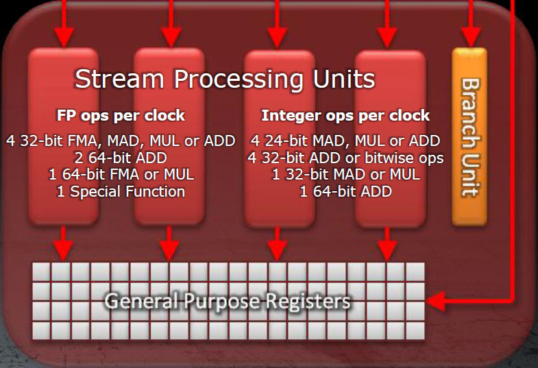
Streamlining the architecture doesn’t make it any less capable. The four stream processors now have identical capabilities, absorbing the special function unit’s role as well. In its VLIW4 configuration, each stream processor can do:
- Four 32-bit FP FMA, MAD, MUL, or ADD per clock
- Two 64-bit FP ADD per clock
- One 64-bit FP FMA or MUL per clock
- One FP Special Function per clock
- Four 24-bit Int MAD, MUL, or ADD per clock
- Four 32-bit Int ADD or bitwise opps per clock
- One 32-bit Int MAD or MUL per clock
- One 64-bit ADD per clock
Moving beyond the GPU’s shading core, its render back-ends are able to handle 16-bit integer ops 2x faster, while 32-bit FP ops are 2x-4x faster. According to AMD, this most directly affects anti-aliasing performance.
Augmenting Compute Performance
Although AMD’s compute-oriented aspirations are often taken less seriously than Nvidia’s, this does sound like an area that received some attention with Cayman. For instance, whereas the Radeon HD 5800-series cards perform double-precision math at one-fifth of the single-precision rate, Cayman operates at one-quarter the SP rate. Although the Radeon HD 6970’s peak single-precision rate is a touch lower than Radeon HD 5870 (2.7 TFLOPS versus 2.72 TFLOPS), you end up with 675 GFLOPS of peak double-precision math on the Radeon HD 6970 compared to 5870’s 544 GFLOPS.
Get Tom's Hardware's best news and in-depth reviews, straight to your inbox.
Note also that the Barts GPU sacrifices DP altogether, focusing on gaming performance rather than compute capabilities.
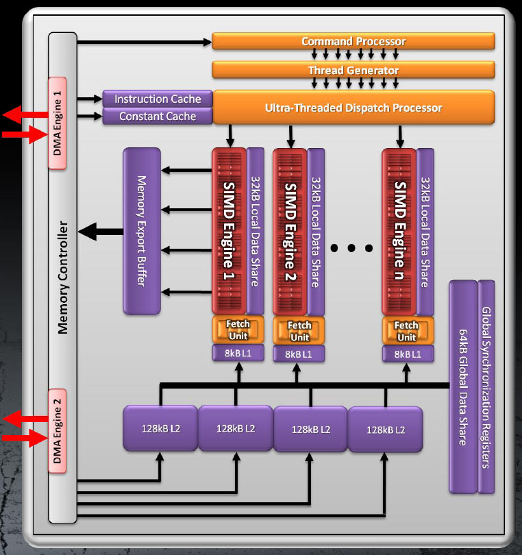
Cayman also incorporates dual bidirectional DMA engines, which ideally yield faster reads and writes to and from system memory over the PCI Express bus.
Finally, AMD gives Cayman the ability to handle independent applications across the GPU. This is in contrast to Fermi, which can handle multiple kernels, so long as they’re spawned from the same CPU thread. Interestingly, that functionality isn’t part of DirectX 11, so AMD has to instead enable it through OpenCL sometime in the future.
Aside from those functionality tweaks, Cayman retains Cypress’ cache structure. Each SIMD has its own 8 KB L1 cache for computational work, aside from the 16 KB L1 texture cache, plus a 32 KB local data share. Four 128 KB L2 caches continue keeping those SIMDs fed with information, and there is still a 64 KB global repository shared by all of the SIMDs.
Current page: Building Cayman By Improving Cypress
Prev Page Radeon HD 6970 And 6950 Arrive Next Page AMD Acknowledges That Geometry Matters-
Annisman Thanks for the review Angelini, these new naming schemes are hurting my head, sometimes the only way to tell (at a quick glance) which AMD card matches up to what Nvidia card, is by comparing the prices, which I think is bad for the average consumer.Reply -
rohitbaran These cards are to GTX 500 series what 4000 series was to GTX 200. Not the fastest at their time but offer killer performance and feature set for the price. I too expected 6900 to be close to GTX 580, but it didn't turn out that way. Still, it is the card I have waited for to upgrade. Right in my budget.Reply -
notty22 AMD's top card is about a draw with the gtx 570.Reply
Pricing is in line.
Gives AMD only hold outs buying options, Nvidia already offered
Merry Christmas -
IzzyCraft Sorry all i read was thisReply
"This helps catch AMD up to Nvidia. However, Intel has something waiting in the wings that’ll take both graphics companies by surprise. In a couple of weeks, we'll be able to tell you more." and now i'm fixated to weather or not intel's gpu's can actually commit to proper playback. -
andrewcutter but from what i read at hardocp, though it is priced alongside the 570, 6970 was benched against the 580 and they were trading blows... So toms has it at par with 570 but hard has it on par with 580.. now im confused because if it can give 580 perfomance or almost 580 performance at 570 price and power then this one is a winner. Sim a 6950 was trading blows with 570 there. So i am very confusedReply -
sgt bombulous This is hilarious... How long ago was it that there were ATI fanboys blabbering "The 6970 is gonna be 80% faster than the GTX 580!!!". And then reality hit...Reply


