Intel Architecture Day 2021: Alder Lake Chips, Golden Cove and Gracemont Cores
Alder Lake Comes to Fore
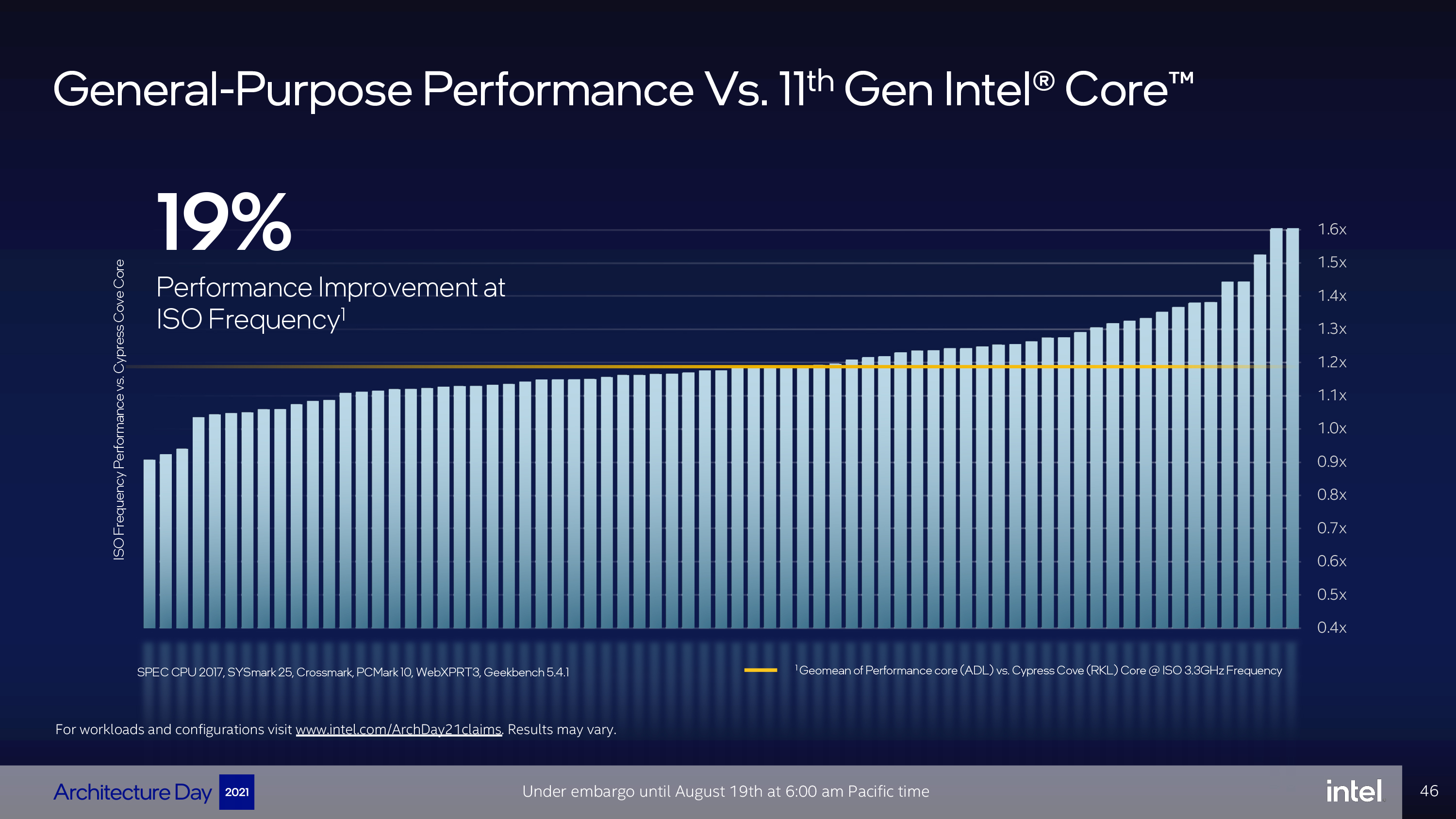
Intel's Architecture Day 2021 was full of deep-dive disclosures, with this year's topics focusing on the architectural details of the company's forthcoming Alder Lake CPUs that will span from the desktop PC down to ultra-mobile applications by combining two types of cores in a hybrid design, a first for an x86 desktop PC chip. However, unlike other Arm hybrid designs we've seen that are tuned for power efficiency, Intel has tuned its Alder Lake chips for the highest performance possible. Intel claims that Alder Lake's high-performance cores come with an average 19% IPC improvement over the Rocket Lake chips, marking the fastest high-performance core the company has built, and that its new efficiency core offers up to five times the power efficiency of Skylake. Intel's Alder Lake also supports features like PCIe 5.0 and DDR5 that leapfrog AMD and Apple in connectivity technology and also outstrip Ryzen's core counts in mobile designs, potentially a much-needed win when Alder Lake comes to market in Fall 2021.
Intel also outlined its Sapphire Rapids and IPU processors for data centers, which bring plenty of radical new advances of their own, and shared details about its new Xe Arc Alchemist discrete gaming GPUs for desktops, along with the datacenter-bound Ponte Vecchio and Xe-HPC GPUs, too.
Intel shared plenty of new information about its latest CPU architectures, but we're focusing on Alder Lake in this article. We've put the short list of disclosures here up front, but we'll drill down in greater depth on each topic in its own section below and on the following pages:
- The Alder Lake SoC will span from desktop PCs to ultramobile devices with TDP ratings from 9W to 125W, all built on the Intel 7 process. The desktop PC comes with up to eight Performance (P) cores and eight Efficient (E) cores for a total of 16 cores and 24 threads and up to 30 MB of L3 cache for a single chip.
- Intel's new hyper-threaded Performance (P) core, which comes with the Golden Cove microarchitecture designed for low-latency single-threaded performance, comes with an average of 19% more IPC than the Cypress Cove architecture in Rocket Lake. It also supports AVX-512 and AMX (a new AI-focused matrix-multiply ISA) for data center variants (both are disabled on consumer chips).
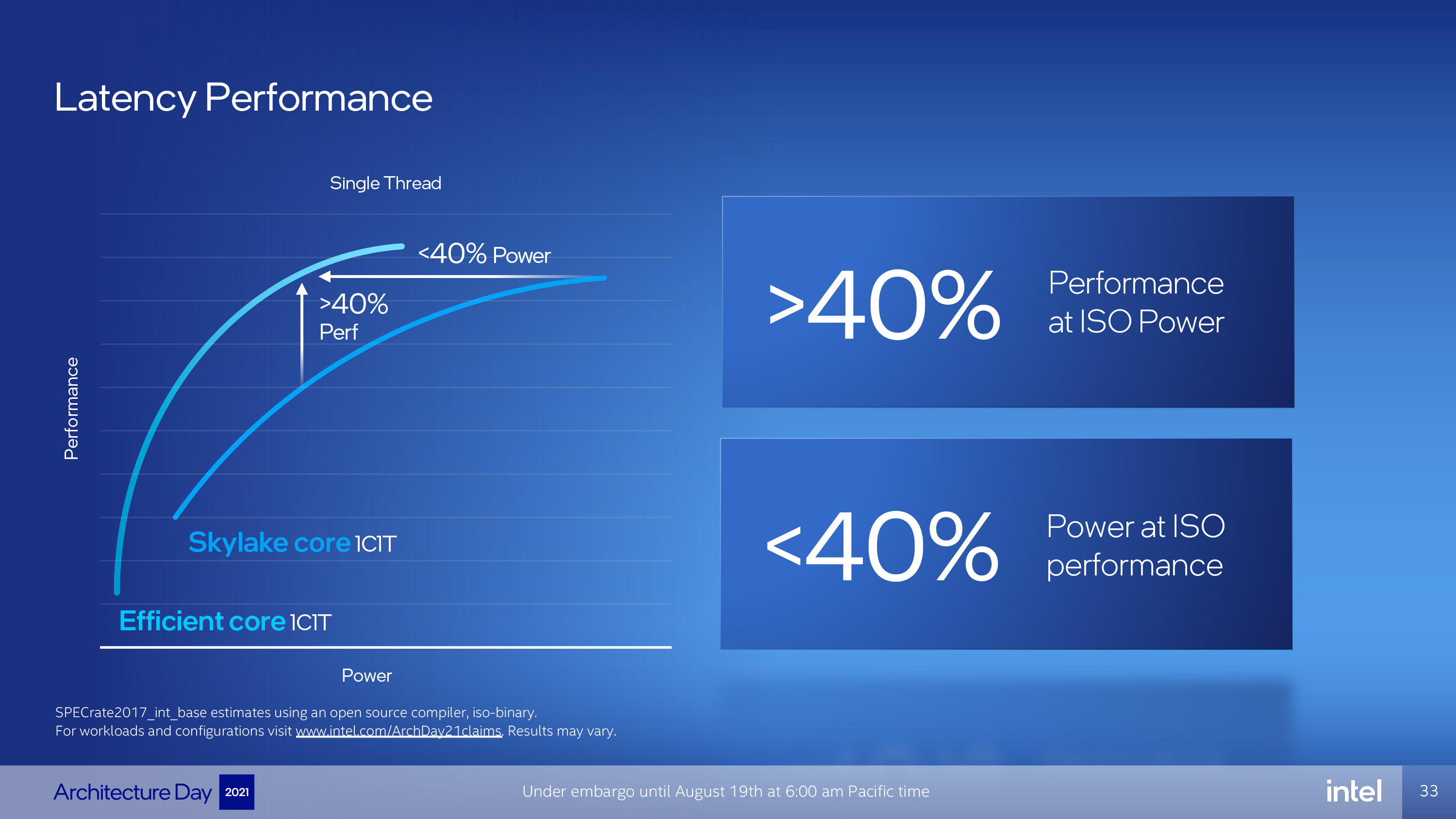
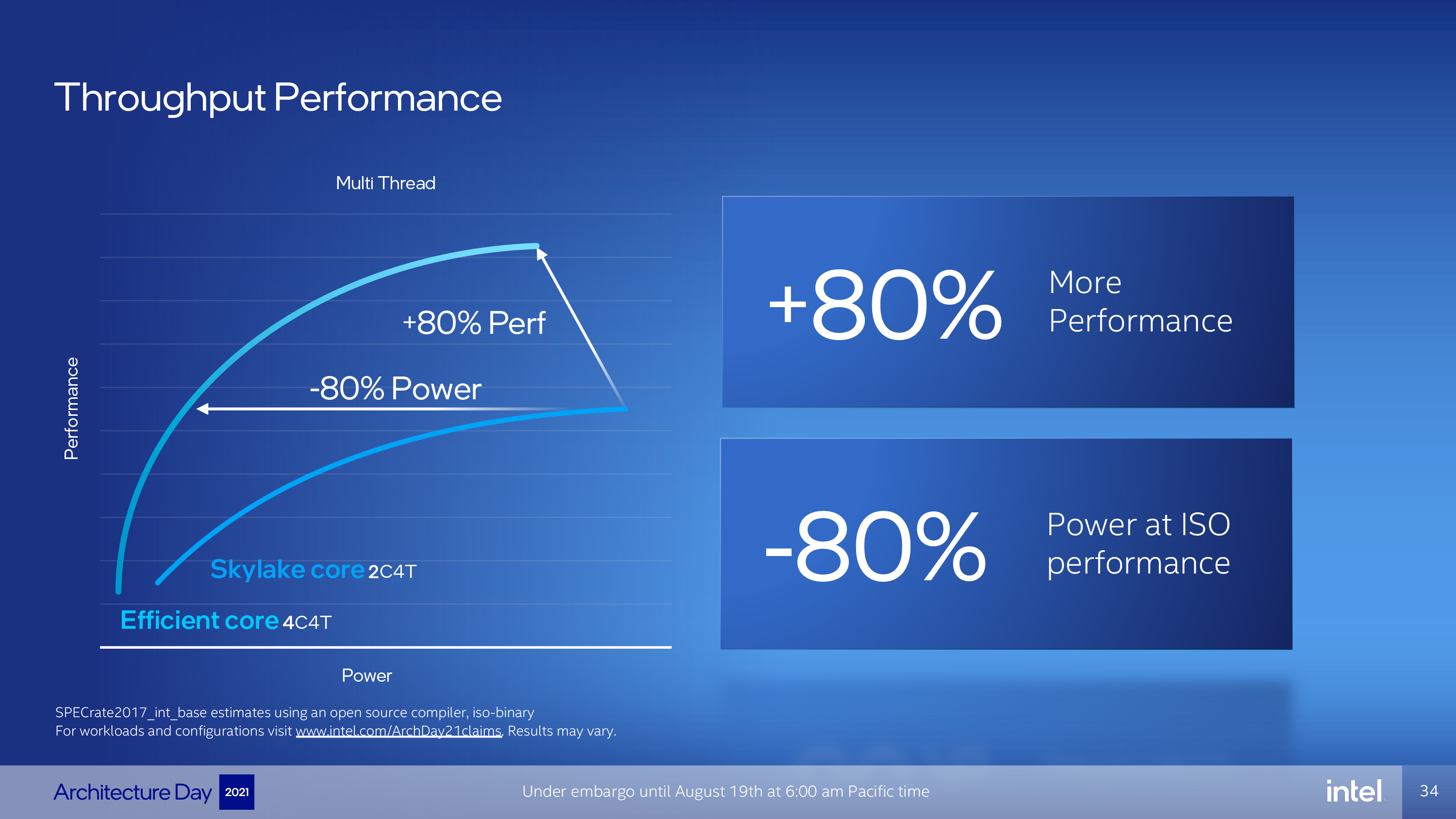
- Intel's new single-threaded Efficiency (E) core, which comes with the Gracemont microarchitecture, is designed to improve multi-threaded performance and provide exceptional area efficiency (small footprint) and performance-per-watt. Four of these small cores fit in the same area as a Skylake core and deliver 80% more performance in threaded work (at the same power). A single E core also delivers 40% more performance than a single-threaded Skylake core (at the same power) in single-threaded work (caveats apply to both).
- Intel's Thread Director is a hardware-based technology that provides enhanced telemetry data to the Windows 11 scheduler to assure that threads are assigned to either the P or E cores in an optimized manner, potentially easing one of the major pain points for a hybrid architecture in a standard desktop environment. This is the sleeper tech that enables the hybrid architecture.
- Alder Lake does not support AVX-512 under any condition (fused off in P cores, not supported in E cores) to ensure an even ISA application.
- Alder Lake supports either DDR4 or DDR5 (LP4x/LP5, too). Desktop PC supports x16 PCIe Gen 5 and x4 PCIe Gen 4, while mobile supports x12 PCIe Gen 4 and x16 PCIe Gen 3, Thunderbolt 4, and Wi-Fi 6E.
- Intel will hold the inaugural Intel Innovation event October 27-28 with keynotes, demos and technical sessions. The event will be both in-person (location unannounced) and remote, and is largely thought to be the official unveiling of the Alder Lake processor stack.
Alder Lake Configurations and SoCs
Quick refresher: Intel's Alder Lake architecture features a design reminiscent of ARM's big.LITTLE, with the larger cores used primarily for high-priority single-threaded work, while the smaller cores execute multi-threaded workloads and less-intensive background tasks. Intel uses a combination of 'big' Performance (P) Golden Cove cores and 'small' Efficiency (E) Atom Gracemont cores for the task. We'll dig deeper into the core architectures on the following pages.
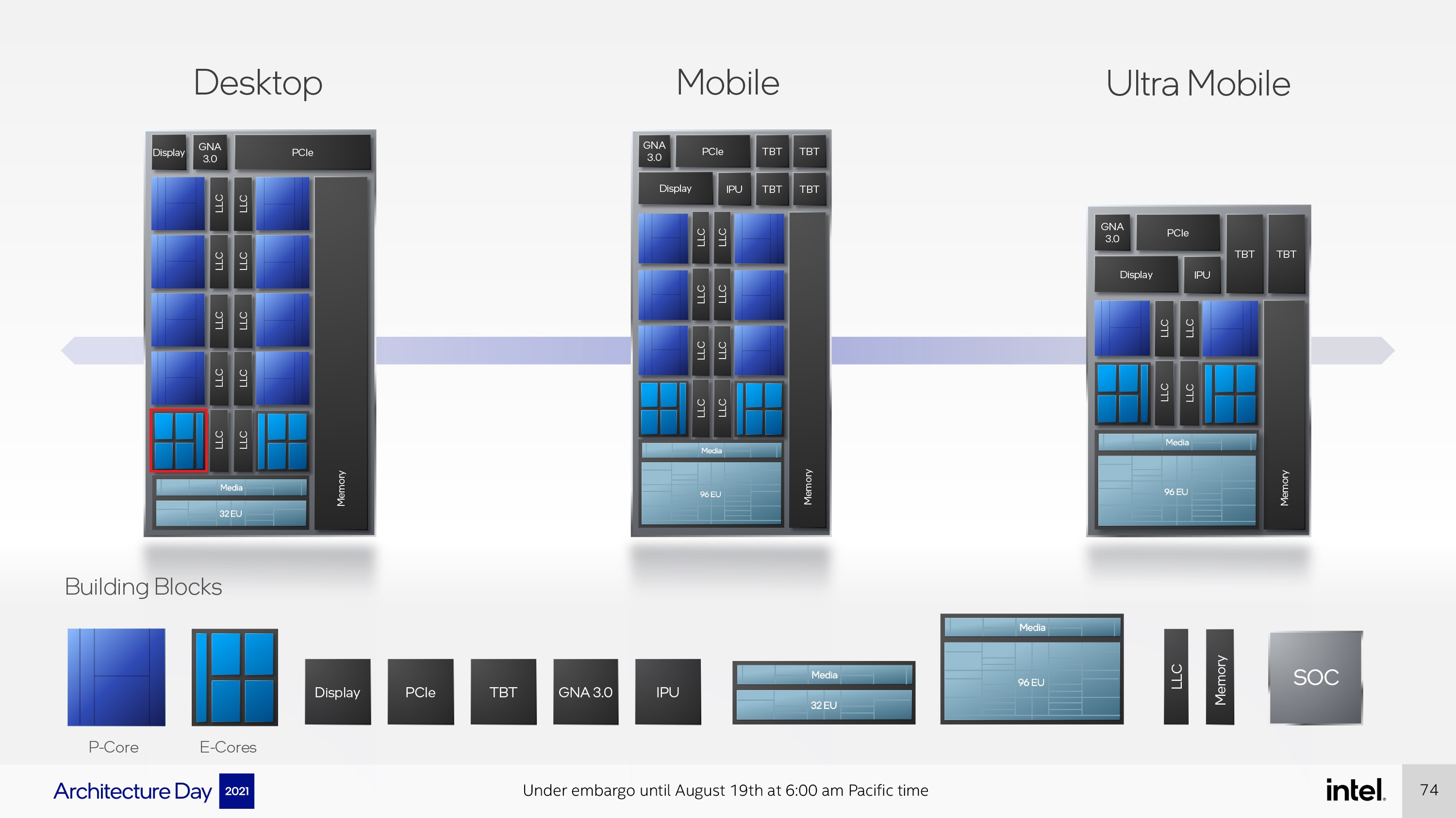
Intel's goal with Alder Lake was to create a handful of IP blocks used to mix-and-match designs that cater to a vast segment of the consumer market spanning from 7W to 125W TDPs.
As you can see above, Intel etches both the P-Cores and E-Cores onto the same single CPU die, with four of the smaller efficient E-Cores (we outlined one E-Core cluster in red) consuming roughly the same amount of die area as a single high-performance P-Core (dark blue). This diagram may not be entirely to scale, but Intel tells us that it can fit four E-Cores into the same amount of space as a single Skylake core.
The Alder Lake chips use the Intel 7 process, which used to be referred to as '10nm Enhanced SuperFin' before Intel recently renamed its process nodes during its latest process and packaging roadmap update. The Golden Cove cores support Hyper-Threading, allowing two threads to run on a single core, while the smaller Gracemont cores are single-threaded. Both types of cores come as part of IP blocks that also include some of the cache topology (like L1, L2, and a portion of LLC). That means some models could come with seemingly odd distributions of cores and threads.
Intel ties the cores, L3 caches (LLC), memory, and other IP blocks together with a ring bus, much like we've seen with its prior CPU architectures for the mainstream desktop.
The media engine, in this case the same Gen12 Xe LP architecture found in Tiger Lake but ported to the Intel 7 process, comes in two variants: one with 32 EUs (GT1) for desktop PCs (because they tend to use discrete GPUs), and another GT2 variant with 96 EUs for the mobile variants. Intel says the Xe LP engine supports 1080p gameplay and features a 12-bit end-to-end video pipeline. You'll notice that the desktop PC models don't have Thunderbolt 4 connectivity or an image processing unit (IPU), with those features being used only for mobile variants.
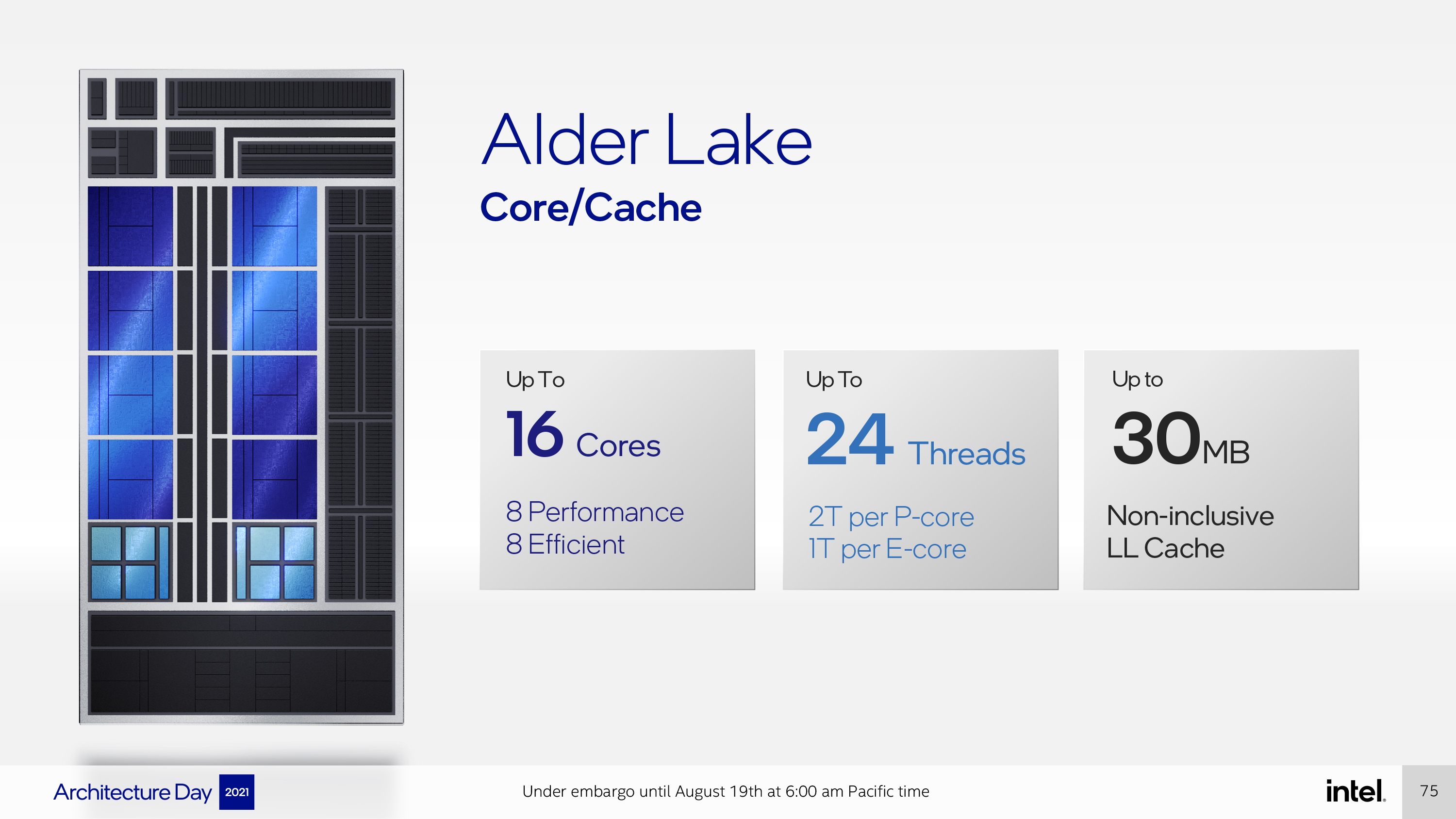
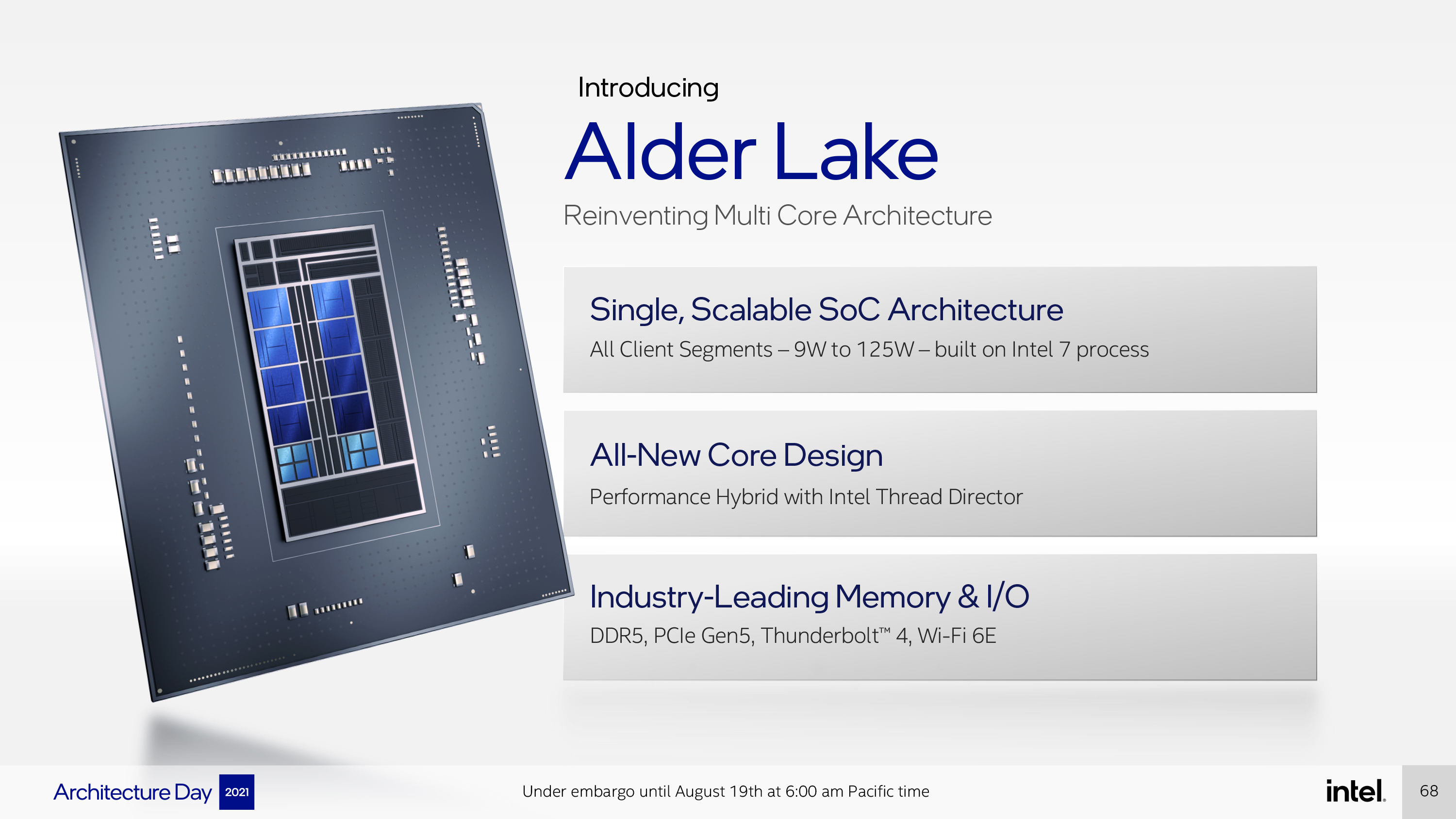
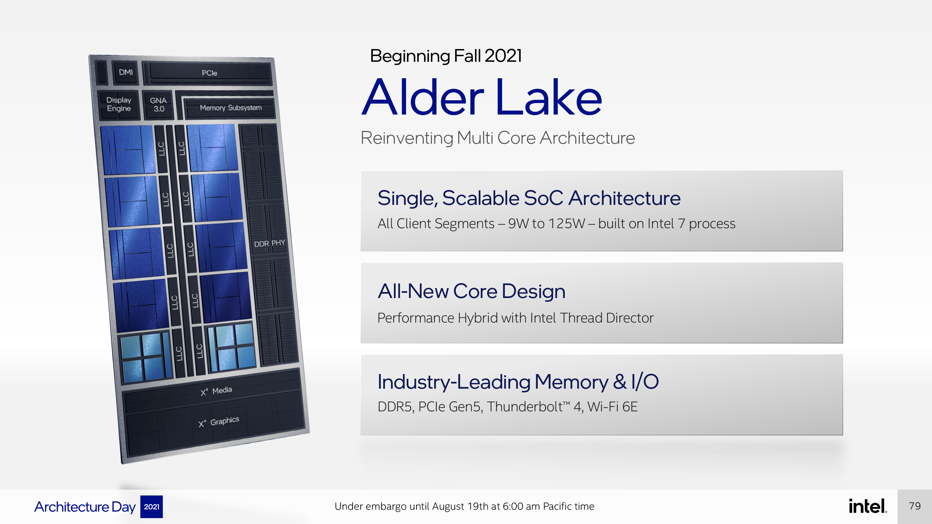
The Alder Lake desktop PC chips will come with a maximum of eight performance cores and eight efficiency cores with a total of 24 threads (two threads per P-Core, one thread per E-Core). These chips will also top out with up to 30MB of L3 cache.
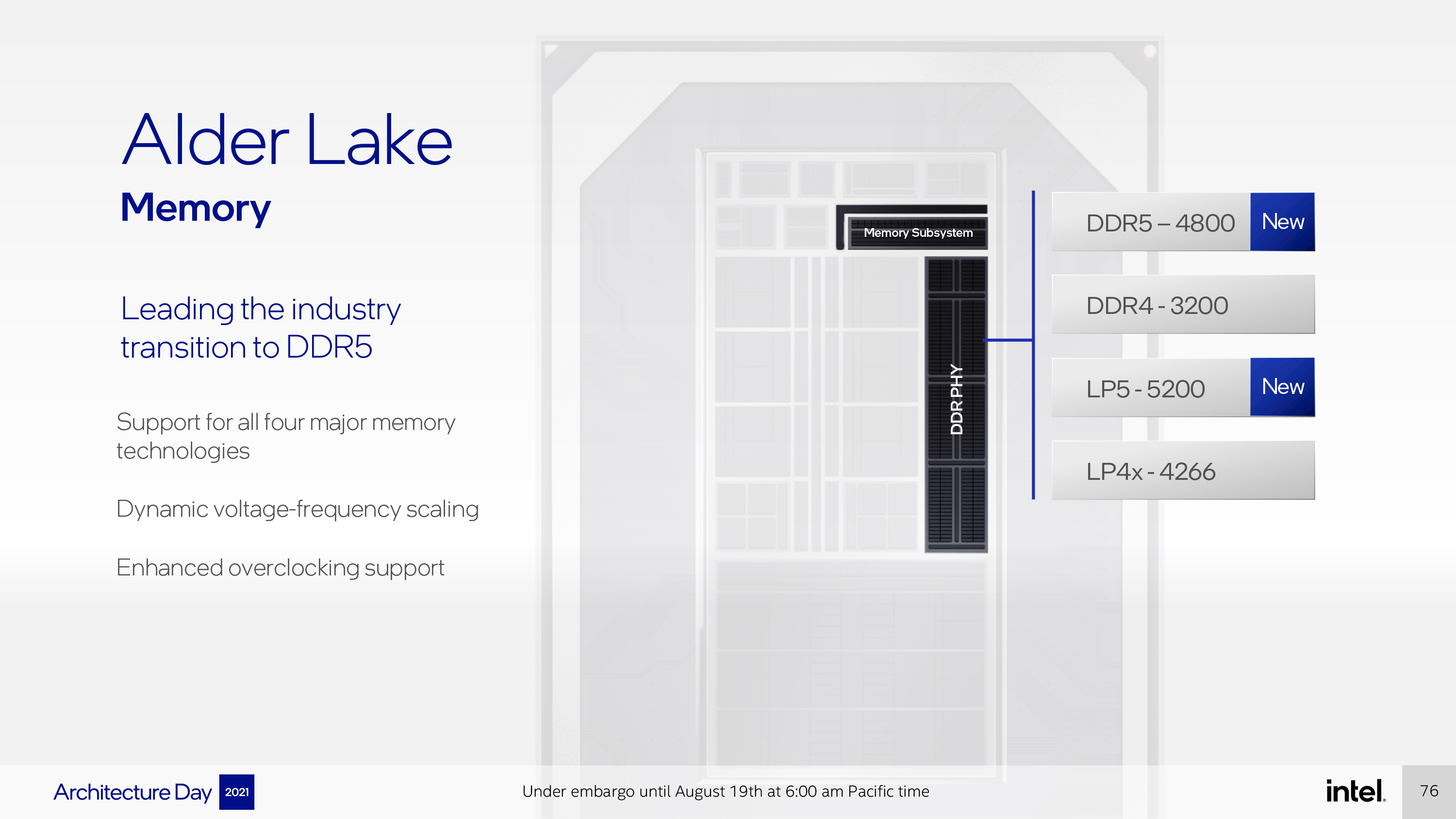
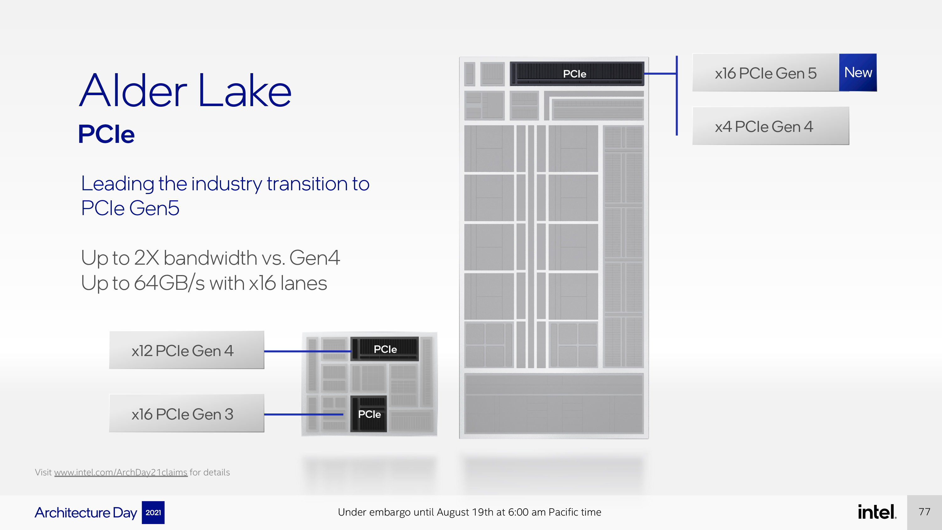
Alder Lake's new memory controllers support four different memory types: DDR5-4800 and LP5-5200, along with DDR4-3200 and LP4x-4266. This single design's broad memory support enables different types of memory configurations for different use-cases. It appears that Intel will split its memory support into DDR4 for lower-end motherboards (B- and H-series motherboards) and mobile systems, while DDR5 will only slot in for higher-end configurations (Z-series motherboards). This makes sense given the expected high pricing for DDR5 memory in the early days of adoption, though it's notable that Intel hasn't confirmed its approach yet.
Alder Lake also supports up to PCIe 5.0 with 64 GB/s of throughput across a x16 lane connection. The desktop PC chips support a x16 PCIe Gen 5 connection with an additional x4 PCIe Gen 4 connection (it is unclear if this x4 connection is used for the chipset or exposed to the user), while lower-power variants support a x12 PCIe Gen 4 config paired with a x16 PCIe Gen 3 connection.
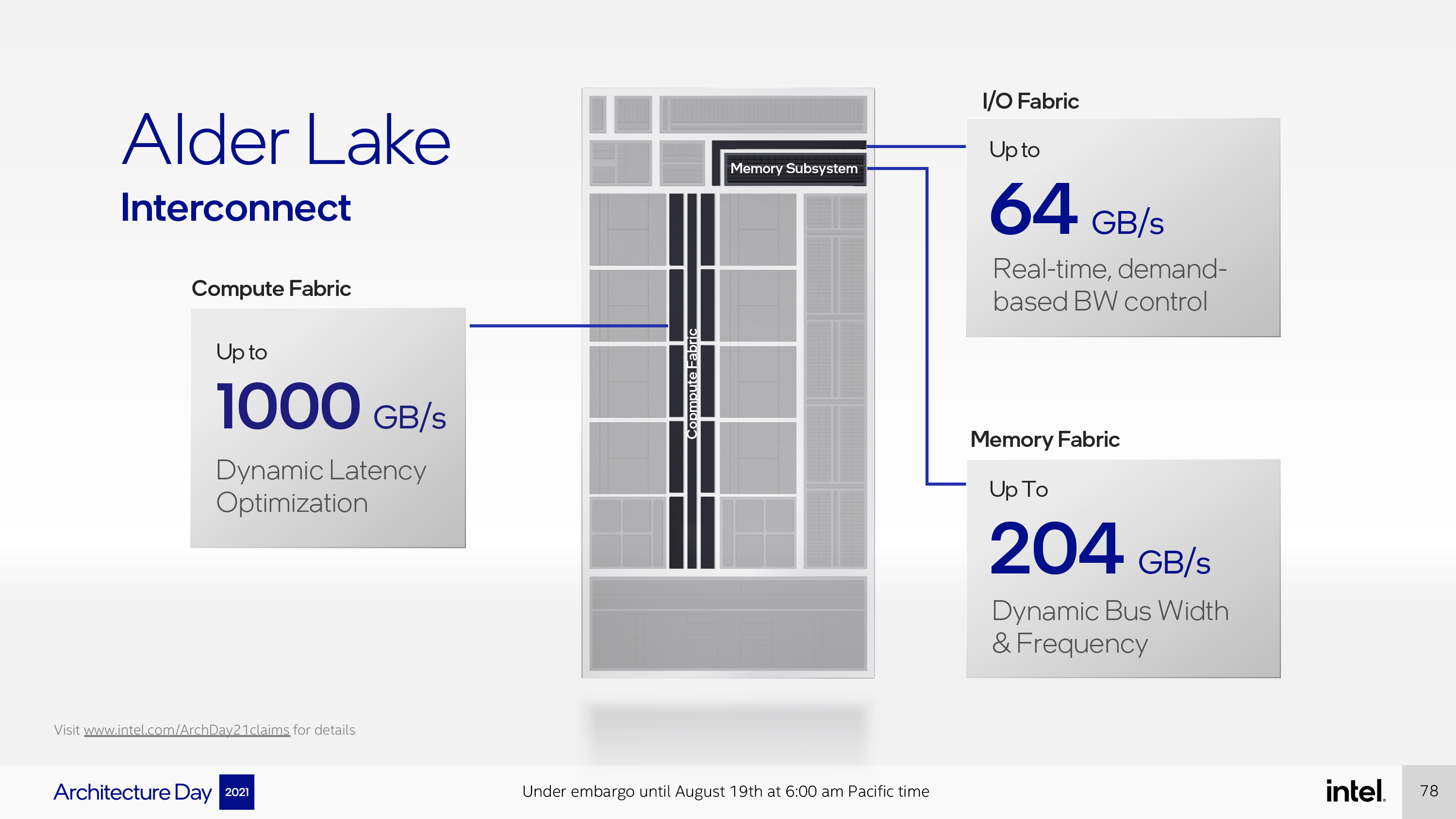
The collection of P and E cores, caches, and higher-throughput 64 GB/s PCIe 5.0 and DDR5 subsystems requires a robust fabric to ensure low-latency high-throughput connections between the various elements. Alder Lake's compute fabric ties these elements together with 1000 GB/s of throughput available across the whole cluster of elements, or even to a single core. Intel says this bus features a dynamic bandwidth/latency optimization scheme based on fabric utilization, but it remains unclear how much this differs from a standard ring bus with its traffic routing mechanisms. This system can also shift the L3 cache from an inclusive or non-inclusive policy based upon utilization.
Additionally, the memory fabric supports up to 204 GB/s of throughput that can be modulated in real time via both bus width and frequency adjustments. This means Alder Lake's memory subsystem can dynamically adjust between higher- and lower-frequency operation states based upon real-time demand-based heuristics workload analysis, with the intent to optimize for power or performance based on the workload at hand.
The first chips based on the design come in three different packages, each for a different segment: The desktop PC chip that will drop into new motherboards with an LGA 1700 CPU socket (yes, 115x coolers with converters are compatible), a high-performance BGA Type3 package for mobile applications (this is likely a 12-28W UP3 package, though Intel hasn't confirmed), and a high-density BGA Type4 HDI package for Ultra Mobile applications (likely a 7-15W UP4 equivalent for ultra-thins).
We've already gleaned plenty of information from official Linux Coreboot patches that outline the various combinations of P- and E-cores, and we've also narrowed down Intel's three product categories in the image above:
- Alder Lake-S: Desktop PCs
- Alder Lake-P: High-performance notebooks
- Alder Lake-M: Low-power devices
| Big + Small Cores | Cores / Threads | GPU |
| 8 + 8 | 16 / 24 | GT1 - Gen12 32EU |
| 8 + 6 | 14 / 22 | GT1 - Gen12 32EU |
| 8 + 4 | 12 / 20 | GT1 - Gen12 32EU |
| 8 + 2 | 10 / 18 | GT1 - Gen12 32EU |
| 8 + 0 | 8 / 16 | GT1 - Gen12 32EU |
| 6 + 8 | 14 / 20 | GT1 - Gen12 32EU |
| 6 + 6 | 12 / 18 | GT1 - Gen12 32EU |
| 6 + 4 | 10 / 16 | GT1 - Gen12 32EU |
| 6 + 2 | 8 / 14 | GT1 - Gen12 32EU |
| 6 + 0 | 6 / 12 | GT1 - Gen12 32EU |
| 4 + 0 | 4 / 8 | GT1 - Gen12 32EU |
| 2 + 0 | 2 / 4 | GT1 - Gen12 32EU |
*Intel has not officially confirmed these configurations. Therefore, not all models may come to market. However, listings assume all models have Hyper-Threading enabled on the large cores.
As we can see above, the flagship desktop PC model would come with eight Hyper-Threading enabled 'big' cores and eight single-threaded 'small' cores, for a total of 24 threads. So logically, we could expect the 8 + 8 configuration to fall into the Core i9 classification, while 8 + 4 could land as Core i7, and 6 + 8 and 4 + 0 could fall into Core i5 and i3 families, respectively. But, naturally, it's impossible to know how Intel will carve up its product stack due to the completely new paradigm of the hybrid x86 design.
Now that we have a much better idea of how the chips are designed at the SoC level, let's see how Intel makes sure applications land on the correct cores, and then take a dive into the core microarchitectures.
Get Tom's Hardware's best news and in-depth reviews, straight to your inbox.
Current page: Intel Unveils Alder Lake
Next Page Intel Alder Lake Thread Director Technology and AVX-512
Paul Alcorn is the Editor-in-Chief for Tom's Hardware US. He also writes news and reviews on CPUs, storage, and enterprise hardware.
-
TerryLaze ReplyAlder Lake does not support AVX-512 under any condition (fused off in P cores, not supported in E cores).
Called it that all they need to do to get power draw down to ryzen levels is to turn off avx.
If they also locked down power limits, at least on non OC boards, they can sell it as super future low power tech. -
JWNoctis No AVX-512 at all?...Yeah, that's gonna be a rather huge regression for those applications that made use of them, which is admittedly uncommon in consumer space.Reply
But then there's not that much difference between Core, Pentium, and Celeron lines anymore, unless they are going to detune IPC in microcode or something. What's the name of the next one, I wonder? -
TerryLaze Reply
Rocketlake didn't get any pentiums or celerons, no reason to believe that alder lake will have them.JWNoctis said:No AVX-512 at all?...Yeah, that's gonna be a rather huge regression for those applications that made use of them, which is admittedly uncommon in consumer space.
But then there's not that much difference between Core, Pentium, and Celeron lines anymore, unless they are going to detune IPC in microcode or something. What's the name of the next one, I wonder?
Now the celeron (atom) is going to be integrated in the core... :p -
Giroro Intel keeps talking up how great their tiny gracemont cores are... But if 4 gracemont cores were able to outperform 1 Golden Cove core, then the entire CPU would be gracemont. I think its no coincidence that their desktop CPUs tacked on exactly enough tiny cores to confuse people into thinking they have parity with 16-core ryzen. Just like how they renamed their 10nm process to give the illusion of parity.Reply
I have no confidence whatsoever that their 8C/8c/24t processor has better multithreaded performance than a hypothetical 10C/0c/20t processor. If that were the case, then the configurations would be more like 0C/40c/40t... Or maybe even 2C/32c/36t.
But no, this is all about how they can technically get away with selling what is essentially an 8 core processor, using a giant sign that says 16 CORES* WORLD'S BEST EFFICIENCY**!
They at least know performance matters a little bit, because a 40 CORE CPU has to got be pretty tempting to somebody in their marketing department, regardless of how bad it would be. -
Johnpombrio This will probably be my next CPU replacing my i9-9900K. I need at least PCI-4.0 for my 2TB Samsung 980 Pro ($313 lightning deal in Amazon Prime day in June). I will never need all of these cores tho.Reply -
mdd1963 Cautiously optimistic, but, I recall feeling the same way before 11th gen released...Reply
This time I will be pessimistic until happily (hopefully) proven wrong. :)
(Need some BF1/BF5 1080P benchmarks to truly know if Alder Lake is 'mo betta'!) -
JamesJones44 ReplyGiroro said:Intel keeps talking up how great their tiny gracemont cores are... But if 4 gracemont cores were able to outperform 1 Golden Cove core, then the entire CPU would be gracemont. I think its no coincidence that their desktop CPUs tacked on exactly enough tiny cores to confuse people into thinking they have parity with 16-core ryzen. Just like how they renamed their 10nm process to give the illusion of parity.
I have no confidence whatsoever that their 8C/8c/24t processor has better multithreaded performance than a hypothetical 10C/0c/20t processor. If that were the case, then the configurations would be more like 0C/40c/40t... Or maybe even 2C/32c/36t.
But no, this is all about how they can technically get away with selling what is essentially an 8 core processor, using a giant sign that says 16 CORES* WORLD'S BEST EFFICIENCY**!
They at least know performance matters a little bit, because a 40 CORE CPU has to got be pretty tempting to somebody in their marketing department, regardless of how bad it would be.
How do you explain M1s multi thread performance then, the quote makes little sense. There is a lot more to CPU design than the number of cores and their single thread IPC. I don't claim to know if they will be able to compete with a 10 big core CPU, but the M1 and other hybrid architectures prove that very good multi thread performance can be had with the big little design. -
ezst036 ReplyGiroro said:I think its no coincidence that their desktop CPUs tacked on exactly enough tiny cores to confuse people into thinking they have parity with 16-core ryzen. Just like how they renamed their 10nm process to give the illusion of parity.
There may be some of that, but Intel at this point can afford to cede some of the high end to AMD. They don't have to outright win, they just have to be competitive enough. And Intel is also prepping to fight AMD as well on the GPU front.(also nVidia)
Intel's biggest threat is ARM. They cannot afford to keep taking it on the chin any longer in mobile. Alder Lake big.little will be a game changer even if it doesn't get the final mile to energy efficiency utopia.
But really, I think people also forget or they discount that the pressure from manufacturing also is playing a factor here. Intel's fab woes go back how many years now? Intel needs small cores partially, and manufacturing woes in all sectors of chip manufacturing is going to force AMD to do the same with big.LITTLE. They've got Jaguar or Bobcat or whatever the latest iteration of that little core was, it won't be long before it's tacked on for some AMD big.LITTLE also.
16 big cores is simply more stress on manufacturing than 8 big and 8 small when you factor in the big picture and tons of silicon wafer after wafer after wafer. Alder Lake helps Intel to help Intel out on their fab woes. -
ezst036 ReplyJamesJones44 said:How do you explain M1s multi thread performance then
You only need one word.
Optimization.
Apple controls all aspects of MacOS, and are particularly fans of cutting off their own customers after so many years. They don't want, don't need, and simply don't carry a lot of legacy "baggage" - even if you spent $8000 on your computer. Apple will cut you off.
You explain M1 performance with optimizations under the hood.
