The Myths Of Graphics Card Performance: Debunked, Part 2
Get Tom's Hardware's best news and in-depth reviews, straight to your inbox.
You are now subscribed
Your newsletter sign-up was successful
NVAPI: Measuring Graphics Memory Bandwidth Utilization
Experimenting With Nvidia's NVAPI
Nvidia, through its GeForce driver, exposes a programming interface ("NVAPI") that, among other things, allows for collecting performance measurements. For the technically inclined, here is the relevant section in the nvapi.h header file:
FUNCTION NAME: NvAPI_GPU_GetDynamicPstatesInfoExDESCRIPTION: This API retrieves the NV_GPU_DYNAMIC_PSTATES_INFO_EX structure for the specified physical GPU. Each domain's info is indexed in the array. For example:- pDynamicPstatesInfo->utilization[NVAPI_GPU_UTILIZATION_DOMAIN_GPU] holds the info for the GPU domain. There are currently four domains for which GPU utilization and dynamic P-state thresholds can be retrieved: graphic engine (GPU), frame buffer (FB), video engine (VID), and bus interface (BUS).
Beyond this header commentary, the API's specific functionality isn't documented. The information below is our best interpretation of its workings, though it relies on a lot of conjecture.
Article continues below- The graphics engine ("GPU") metric is expected to be your bottleneck in most games. If you don't see this at or close to 100%, something else (like your CPU or memory subsystem) is limiting performance.
- The frame buffer ("FB") metric is interesting, if it works as intended. From the name, you'd expect it to measure graphics memory utilization (the percentage of memory used). That is not what this is, though. It appears, rather, to be the memory controller's utilization in percent. If that's correct, it would measure actual bandwidth being used by the controller, which is not otherwise available as a measurement any other way.
- We're not as interested in the video engine ("VID"); it's not generally used in gaming, and registers a flat 0% typically. You'd only see the dial move if you're encoding video through ShadowPlay or streaming to a Shield.
- The bus interface ("BUS") metric refers to utilization of the PCIe controller, again, as a percentage. The corresponding measurement, which you can trace in EVGA PrecisionX and MSI Afterburner, is called "GPU BUS Usage".
We asked Nvidia to shed some light on the inner workings of NVAPI. Its response confirmed that the FB metric measures graphics memory bandwidth usage, but Nvidia dismissed the BUS metric as "considered to be unreliable and thus not used internally".
We asked AMD if it had any API or function that allowed for similar measurements. After internal verification, company representatives confirmed that they did not. As much as we would like to, we are unable to conduct similar tests on AMD hardware.
Moving On To The Actual Tests...
Myth: Graphics memory bandwidth utilization and PCIe bus utilization are impossible to measure directly.
The amount of data moved between graphics memory to the graphics processor and back is massive. That's why graphics cards need such complex memory controllers capable of pushing tons of bandwidth. In the case of AMD's Radeon R9 290X, you're looking at up to 320GB/s. Nvidia's GeForce GTX 780 Ti is rated for up to 336GB/s. Maximum PCIe throughput isn’t as impressive (15.75GB/s through a 16-lane third-gen link), though it isn’t in as much demand. But how much of that is utilized at any given point in time? Is this a bottleneck? Until now, it has been hard to answer those questions. But the Kepler architecture and NVAPI make it possible to address them with more precision, we hope.
Get Tom's Hardware's best news and in-depth reviews, straight to your inbox.
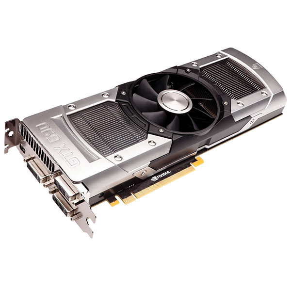
We began our exploration looking at the BUS metric on a GeForce GTX 690. While Nvidia says it’s unreliable, we still wondered what we could glean from our test results. As we took readings, however, we faced another complication: the card's two GK104 GPUs are not linked directly to the main PCIe bus, but are rather switched through a PLX PEX 8747. So, no matter what setting the motherboard uses, the GPUs always operate at PCI Express 3.0 signaling rates, except when they're power-saving. That's why GPU-Z shows them operating at PCIe 3.0, even on platforms limited to PCIe 2.0. The PEX 8747 switch is what drops to previous-gen rates on the host side.
With each GPU's bus controller operating at PCIe 3.0 on a 16-lane link, utilization at 100% should be 15.75GB/s. That information alone doesn't help us much, though. It's impossible to say how much traffic is directed at the host and how much goes to the other GPU. And unfortunately, the PLX switch doesn't give us access to more granular data. For now, we're left with a worst-case scenario: that each GPU is receiving all of its traffic from the host, and none is multicast.
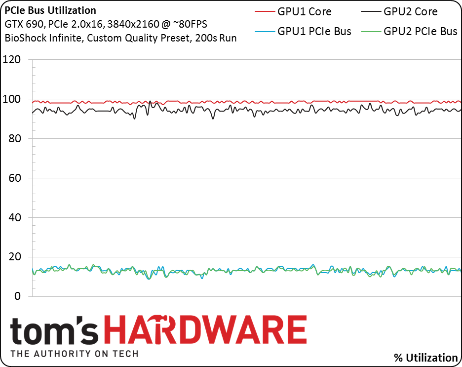
With that explanation, check out the graph above. It is a 200-second run of BioShock: Infinite at a custom quality setting, using a grueling 3840x2160 to average 80 FPS. PCIe bus utilization is in the ~15% range for each of the two GK104s. Even in the academic worst-case situation described above, we're using about ~30% of a 16-lane PCIe 3.0 link, or ~60% of 16 second-gen lanes. And that's a brutal scenario, where 663.6 million pixels per second are being rendered (3840x2160 * 80 FPS) across two GPUs in SLI on a single board. For comparison, 1920x1080 * 60 FPS is 124.4 million pixels per second.
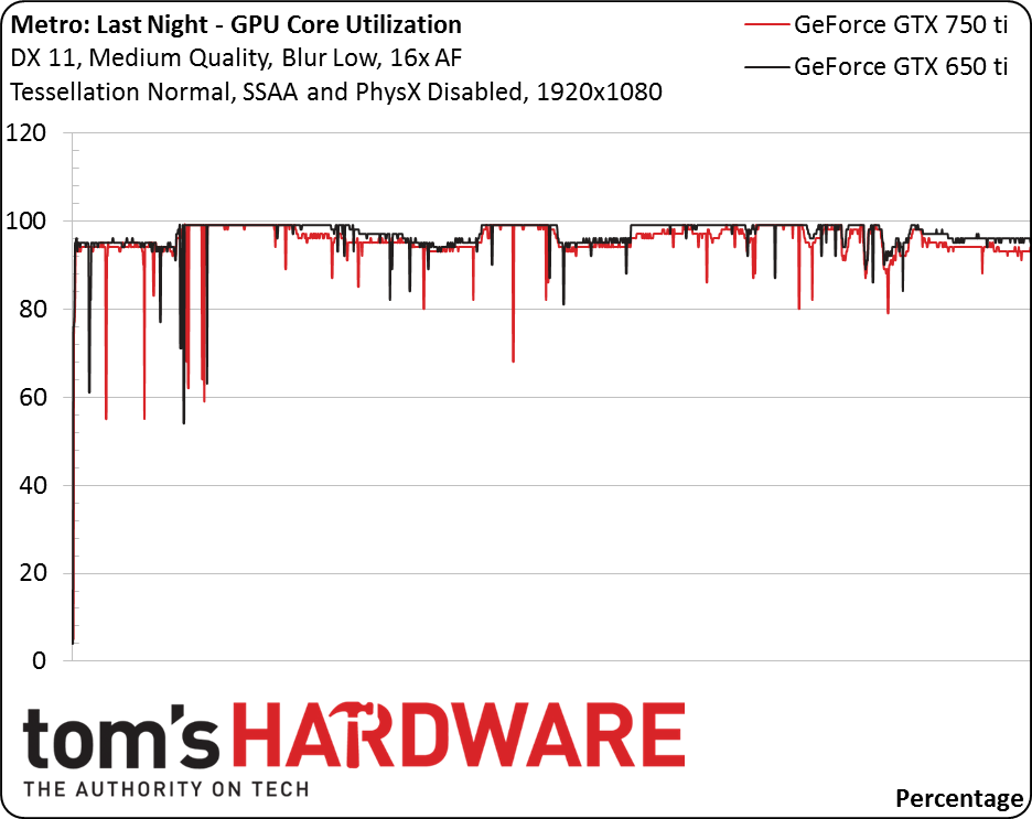
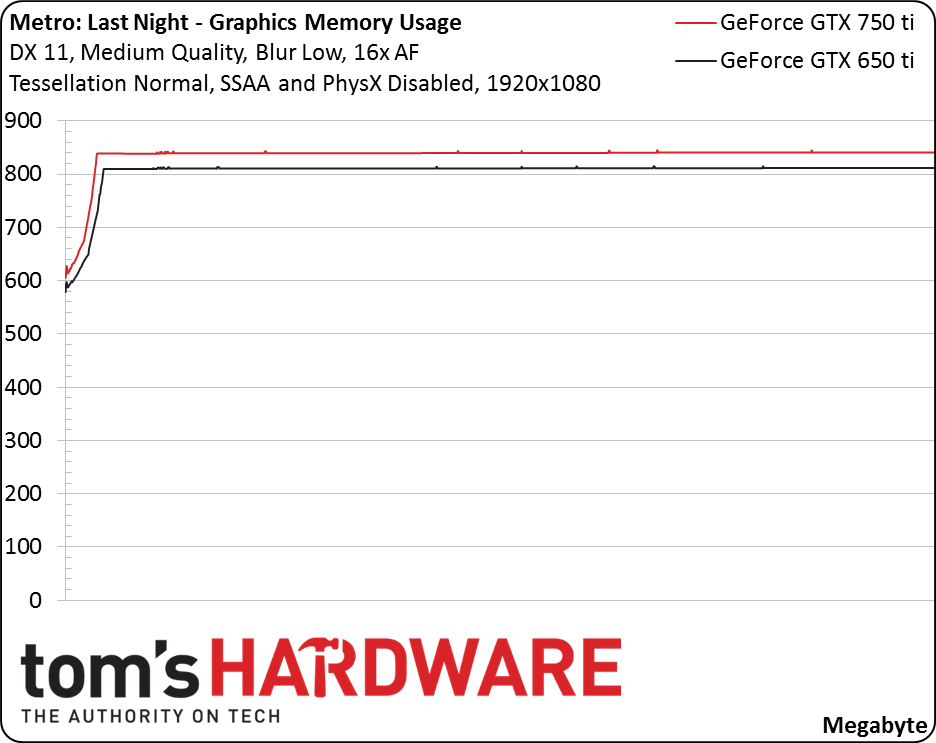
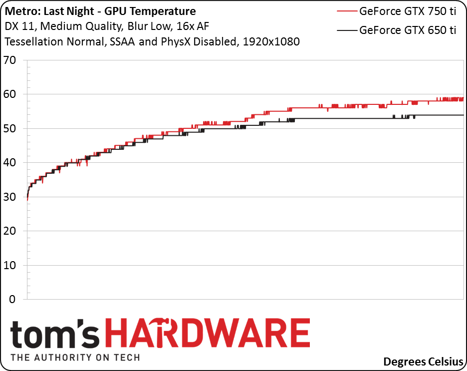
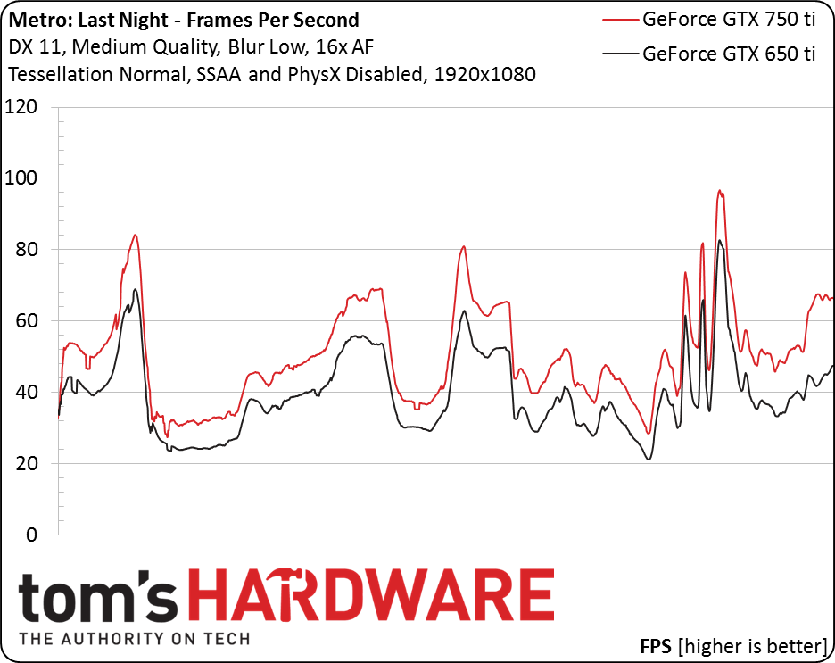
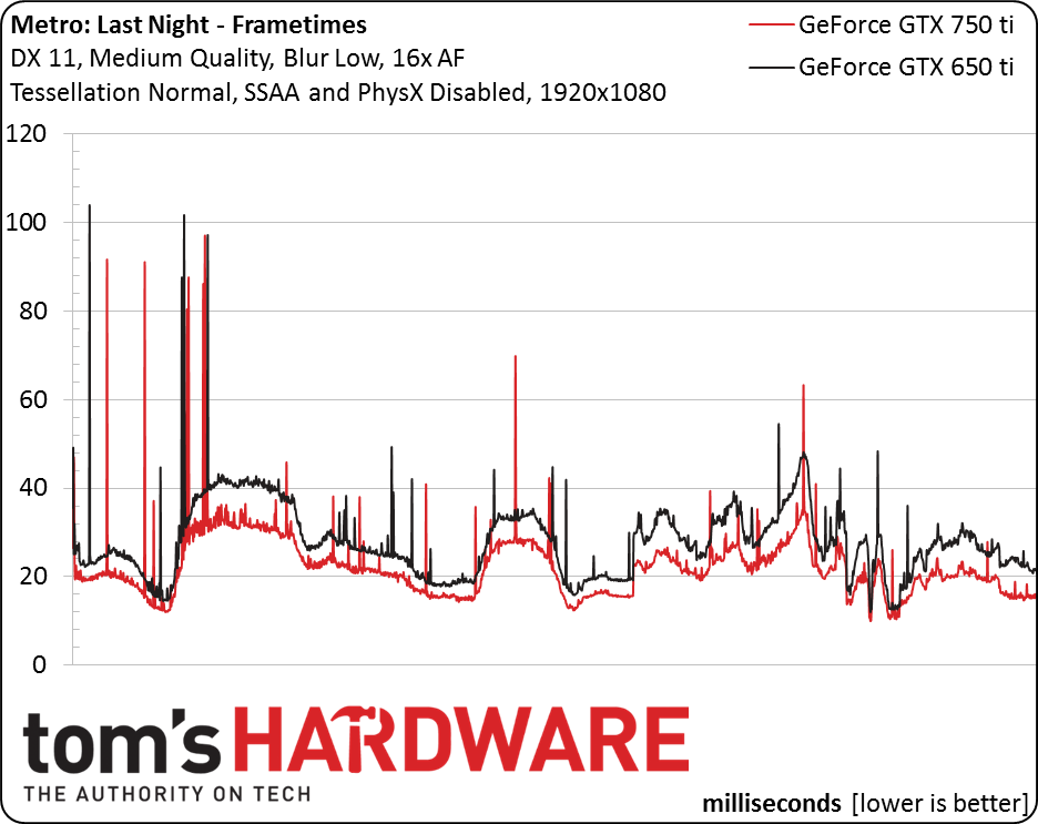
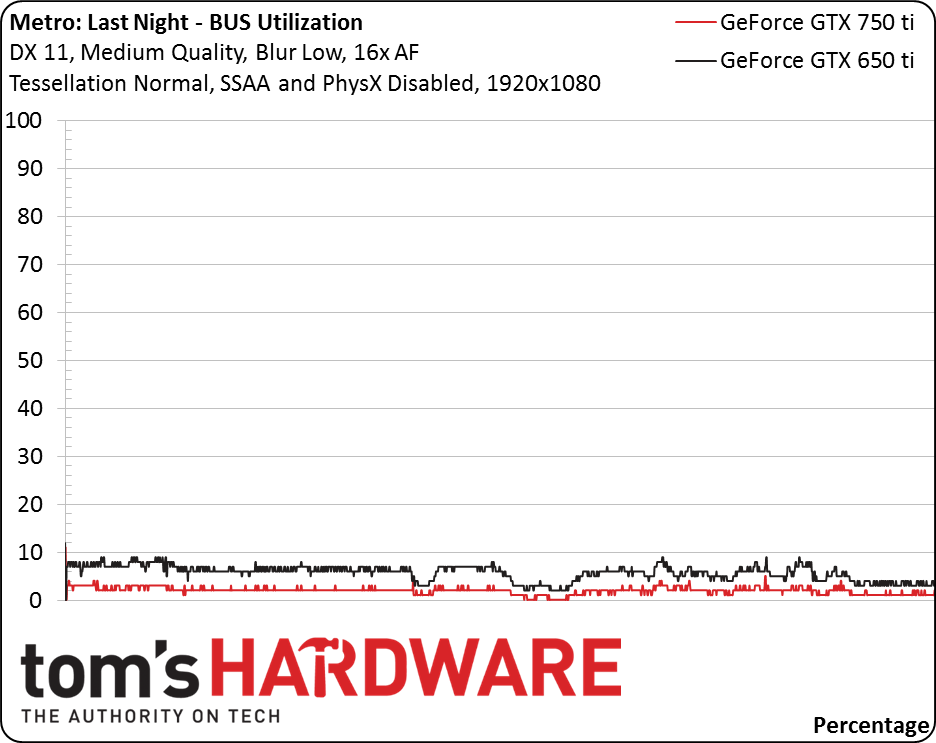
Given the shortcomings of my current hardware selection, I won't go any further with the GeForce GTX 690. Instead, let's proceed to more meaningful tests conducted on a GeForce GTX 750 Ti and the GeForce GTX 650 Ti it replaces. The seven charts that follow may seem like data overload. But they really do need to be considered together. In them, you'll see runs of the Metro: Last Light benchmark using the two aforementioned cards operating on the same platform.
Starting from the first graph, in order, we have: GPU core utilization (%), graphics memory utilization (MB), GPU core temperature (Celsius), frames per second, frame time (milliseconds), "FB" utilization (%) and "BUS" utilization (%). We're omitting core and memory clock rates; they were fixed at their respective GPU Boost values on both cards.
GPU utilization shows that the graphics processor on both cards is the primary system bottleneck. It's close to 100% most of the time. This is as we'd expect, and easy to explain. The GPU core is the component you'd expect a game to tax most heavily.
Graphics memory utilization appears stable under 1GB, which is what the GeForce GTX 650 Ti includes. There's nothing special to report, overall.
GPUs predictably warm up with use. Both of these test subjects remain quite cool compared to enthusiast-class cards, though.
Frame rates are typically what gamers look at, and we can see the GeForce GTX 750 Ti is faster than the 650 Ti. We're not necessarily interested in average FPS in this experiment, but will need relative frame rate as a measure of throughput for an adjustment we'll make later.
The spikes in frame times increase frame time variance. Those spikes coincide with higher (and not lower) frame rates, and with lower (not higher) GPU utilization. This could be the smoking gun of a platform bottleneck (although in this case, not a major one, since GPU utilization remains in the ~95% range; if the platform bottleneck was severe, utilization would drop much more). Still, while that's interesting, we aren't where we want to be with our experiment.
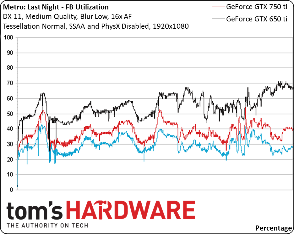
This is one of the new metrics enabled by the NVAPI queries: "FB" or "Framebuffer" Utilization. It's expressed as a percentage, and is actually named misleadingly. What it really measures is the percentage of time each GPU's memory controller is busy and, by proxy, its bandwidth utilization.
Now, we didn't pick these two cards at random. We chose them because they come equipped with the same 128-bit interface at 1350MHz, delivering up to 86.4GB/s. At an equal throughput (FPS), their bandwidth utilization should be directly comparable. Their frame rates aren't the same, though. The GeForce GTX 750 Ti achieves higher performance, shown by the frame rate chart. Thus, we normalize the metric for the GM107-based board using the GeForce GTX 650 Ti's performance. That is the third blue line you see in the chart.
The results are impressive. A Maxwell-based GPU appears to deliver 25% more FPS than a Kepler GPU in the same price range, while at the same time reducing its memory bandwidth utilization by 33%. Stated differently, on a per-frame basis, the GeForce GTX 750 Ti needs half of the memory bandwidth in the Metro: Last Light benchmark.
This fact may have profound implications for the GeForce GTX 980 and 970. Memory interface area can be sacrificed for additional SMM area, bringing power to bear where it's most needed, or to shrink die size, reducing cost.
Our final graph shows, for the first time, directly (versus indirectly via FPS measurements), how extraordinarily small PCIe bandwidth requirements are for a modern graphics card (assuming the readings are meaningful and not "unreliable" as Nvidia says). PCI Express 2.0 gave us 8GB/s of bi-directional throughput from 16-lane links. Both cards fail to hit 10% of that, requiring a sustained figure under 0.8GB/s. That is a mere 5% of what you have available to a single card on a Haswell-based platform.
Graphics Memory Bandwidth Conclusions
Our tests confirms two things:
- Graphics memory bandwidth is not a bottleneck (at least in Metro with a GeForce GTX 750 Ti/650 Ti).
- Graphics memory utilization improvements linked to the Maxwell architecture are beyond impressive - graphics memory bandwidth requirements are essentially halved by Maxwell. This latter finding was confirmed by Nvidia.
The huge reduction in memory bandwidth needs has broad architectural implications, we believe. We're expecting to see (comparatively) smaller graphics memory controllers and the recovered die area put to good use in the form of additional SMMs, further increasing efficiency and performance gains of Maxwell over Kepler.
We'd love to make similar comparisons on AMD cards in the future, should the company enable common functionality in its drivers.
Current page: NVAPI: Measuring Graphics Memory Bandwidth Utilization
Prev Page Testing PCIe At x16/x8 At Three Generations, From 15.75 To 2GB/s Next Page HDTVs, Display Size And Anti-Aliasing-
iam2thecrowe i've always had a beef with gpu ram utillization and how its measured and what driver tricks go on in the background. For example my old gtx660's never went above 1.5gb usage, searching forums suggests a driver trick as the last 512mb is half the speed due to it's weird memory layout. Upon getting my 7970 with identical settings memory usage loading from the same save game shot up to near 2gb. I found the 7970 to be smoother in the games with high vram usage compared to the dual 660's despite frame rates being a little lower measured by fraps. I would love one day to see an article "the be all and end all of gpu memory" covering everything.Reply
Another thing, i'd like to see a similar pcie bandwidth test across a variety of games and some including physx. I dont think unigine would throw much across the bus unless the card is running out of vram where it has to swap to system memory, where i think the higher bus speeds/memory speed would be an advantage. -
blackmagnum Suggestion for Myths Part 3: Nvidia offers superior graphics drivers, while AMD (ATI) gives better image quality.Reply -
chimera201 About HDTV refresh rates:Reply
http://www.rtings.com/info/fake-refresh-rates-samsung-clear-motion-rate-vs-sony-motionflow-vs-lg-trumotion -
photonboy Implying that an i7-4770K is little better than an i7-950 is just dead wrong for quite a number of games.Reply
There are plenty of real-world gaming benchmarks that prove this so I'm surprised you made such a glaring mistake. Using a synthetic benchmark is not a good idea either.
Frankly, I found the article was very technically heavy were not necessary like the PCIe section and glossed over other things very quickly. I know a lot about computers so maybe I'm not the guy to ask but it felt to me like a non-PC guy wouldn't get the simplified and straightforward information he wanted. -
eldragon0 If you're going to label your article "graphics performance myths" Please don't limit your article to just gaming, It's a well made and researched article, but as Photonboy touched, the 4770k vs 950 are about as similar as night and day. Try using that comparison for graphical development or design, and you'll get laughed off the site. I'd be willing to say it's rendering capabilities are actual multiples faster at those clock speeds.Reply -
SteelCity1981 photonboy this article isn't for non pc people, because non pc people wouldn't care about detailed stuff like this.Reply -
renz496 Reply14561510 said:Suggestion for Myths Part 3: Nvidia offers superior graphics drivers
even if toms's hardware really did their own test it doesn't really useful either because their test setup won't represent million of different pc configuration out there. you can see one set of driver working just fine with one setup and totally broken in another setup even with the same gpu being use. even if TH represent their finding you will most likely to see people to challenge the result if it did not reflect his experience. in the end the thread just turn into flame war mess.
14561510 said:Suggestion for Myths Part 3: while AMD (ATI) gives better image quality.
this has been discussed a lot in other tech forum site. but the general consensus is there is not much difference between the two actually. i only heard about AMD cards the in game colors can be a bit more saturated than nvidia which some people take that as 'better image quality'. -
ubercake Just something of note... You don't necessarily need Ivy Bridge-E to get PCIe 3.0 bandwidth. Sandy Bridge-E people with certain motherboards can run PCIe 3.0 with Nvidia cards (just like you can with AMD cards). I've been running the Nvidia X79 patch and getting PCIe gen 3 on my P9X79 Pro with a 3930K and GTX 980.Reply -
ubercake Another article on Tom's Hardware by which the 'ASUS ROG Swift PG...' link listed for an unbelievable price takes you to the PB278Q page.Reply
A little misleading.
