A Third Type Of Processor For VR/AR: Movidius' Myriad 2 VPU
There is a whole new market that is a sea of lava, gurgling to the surface, about to blow the top off of a mountain. It’s virtual and augmented reality, and it’s not just marquee HMDs like the Oculus Rift and HTC Vive and Microsoft HoloLens. It’s dozens of VR/AR headsets and glasses, hundreds of apps and experiences, and new technologies that are being developed to enable and support all of it.
Earlier this year at Microsoft Build, I got a chance to try out the Microsoft HoloLens. My time with it was woefully short, and even after getting a chance to see how the thing works, no one is especially privy to what’s inside it, what makes it tick.
Then, as now, there’s so much we don’t know. But what we do know is that there is an additional, new type of processor in the HoloLens. This, and other VR/AR devices, make heavy use of sensors, and something has to handle all that data.
More Processing, Please
CPUs and GPUs have served us all well, in everything from desktop computers to smartphones and beyond, but Movidius contends that the new computing paradigms presented by VR/AR, drones, smart robots and even the Internet of Things require a third type of processor to work alongside them.
Where Microsoft calls its extra processor an “HPU” (holographic processing unit), Movidius is building a “VPU” (vision processing unit).
Movidius is a “vision sensing” company, and it does not intend to miss the VR/AR bus. It wants to be inside of VR/AR, figuratively and literally. Its next big product is the Myriad 2, a dedicated VPU package (hardware and software) designed to bring “visual intelligence to our machines.”
The Myriad 2 seems destined primarily for mobile devices, which, if you think about it, is more or less the “killer” application -- smart glasses, VR HMDs (which in many cases are designed to be untethered and portable), and even mobile AR solutions like Project Tango. (For that matter, high-end smartphones could benefit from a VPU, especially those designed to work with VR HMDs.)
Get Tom's Hardware's best news and in-depth reviews, straight to your inbox.
To boil it down, Movidius explained the point of the VPU by noting that it’s no longer sufficient to render a complex scene as a GPU does; the device must understand it. That’s just a different beast. Company representatives told Tom’s Hardware in a briefing that cramming that much performance into a low-power SoC was not previously possible and required offloading complex processing to servers in the cloud. The continuing advance of technology, coupled with specialized processors like the Myriad 2 VPU, are allowing these calculations to be done on device, eliminating network latency and enabling new experiences.
The Myriad 2
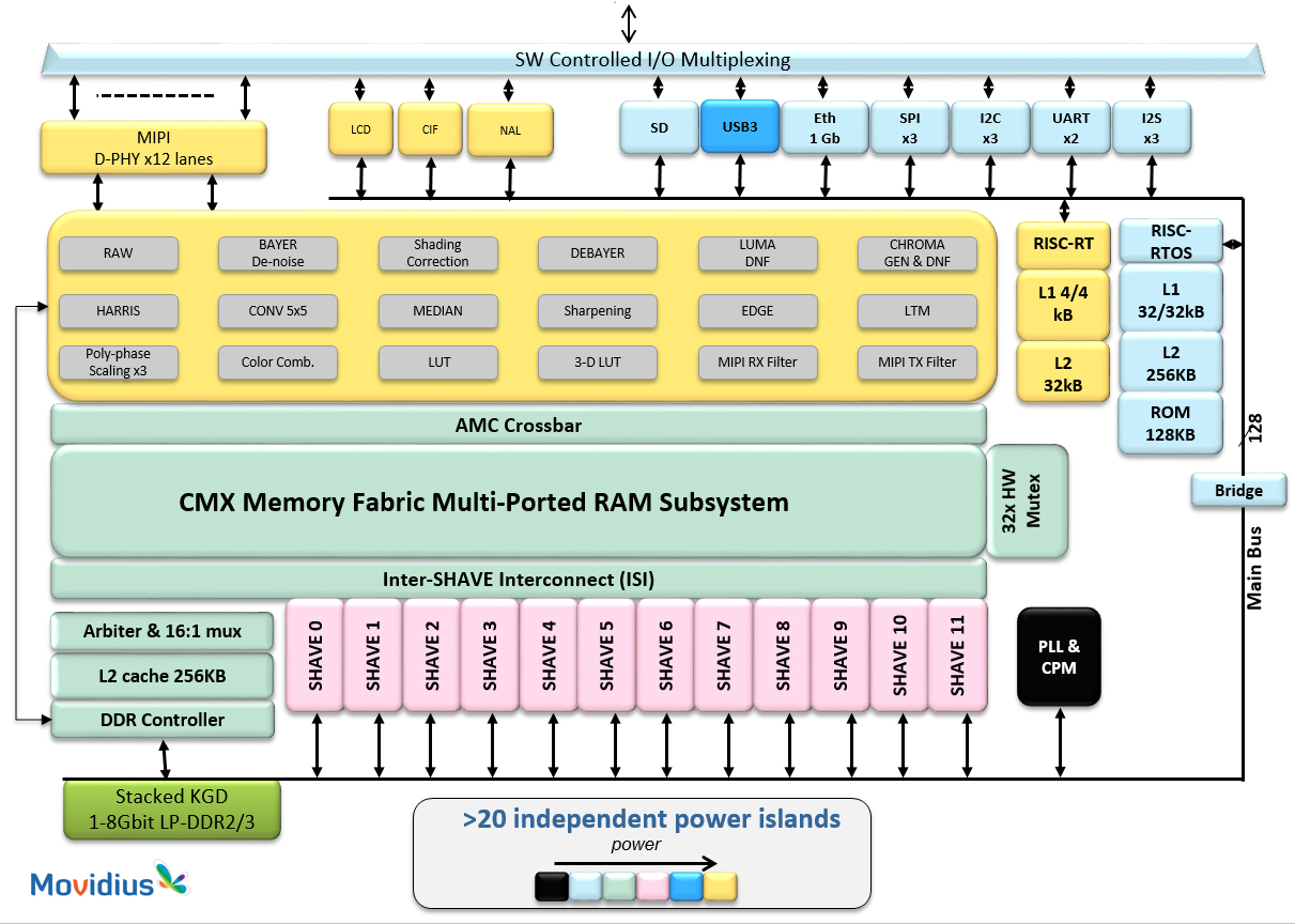
The Myriad 2 vision processor is designed to handle very specific tasks such as eye and gesture tracking, object classification and tracking, and environment mapping. It can process input from up to six HD cameras, which paves the way for stereo depth sensing or multi-directional viewing.
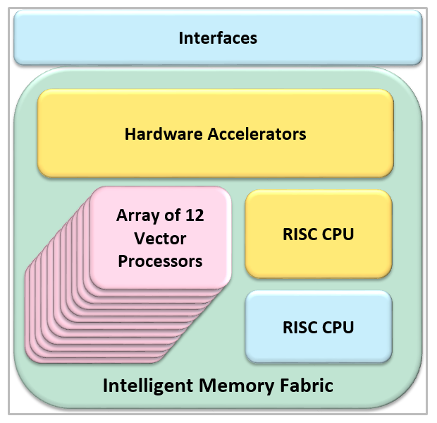
As with other SoCs, the Myriad 2 bundles several different components into one piece of silicon. One of the blocks that's crucial for reducing power consumption includes about 20 fixed-function hardware accelerators for common image processing algorithms that handle noise filtering, sharpening, and so on with an ASIC-style design.
The twelve homegrown (that is to say, proprietary) SHAVE 128-bit SIMD vector units are what provide the processing power at the heart of this VPU. For comparison, a low-power, general purpose CPU such as an ARM Cortex-A57 or -A72 contains two NEON 128-bit SIMD vector units. GPUs also excel at processing highly parallel tasks and are used for many of the same visual processing applications targeted by the Myriad 2. According to Movidius, though, its VPU offers better performance than competing GPUs like Nvidia's Tegra K1 at vision-specific tasks, because its SHAVE vector units support predicated instructions that handle code branches more efficiently. Visual processing is inherently unpredictable, and many algorithms, like those used for edge detection, have interdependencies with surrounding pixels, creating branch-heavy code streams.
The Myriad 2 also contains two different RISC CPUs. Both appear to be SPARC Leon cores, with the smaller of the two dedicated to scheduling within the SoC and the larger core dedicated to running user code within a real-time operating system (RTOS). There's technically no L3 cache for the CPUs, but there is 2 MB of on-chip memory that functions like a hybrid L3 cache, shared between the CPUs, SHAVE vector units, and fixed-function accelerators. This shared memory design avoids the power penalty of moving data between processor islands. The VPU also supports up to 1 GB of additional off-chip DRAM.
I/O support includes SD, USB 3.0 and gigabit Ethernet, as well as UART (x2), SPI (x3), and I2C (x3) and I2S (x3). The Myriad 2 uses a MIPI interface with twelve lanes. A Movidius rep said that this way, data can enter sit in main memory while it’s operated on. This, he said, is in contrast to traditional SoC architectures, where each port tends to have its own buffer, which he said wastes a lot of power moving data between buffers and memory.
The clock speed will be between 300-600 MHz with a power envelope of less than 2 W (at 500 MHz it should draw just 1.5 W). The total package size is 5 x 5 x 0.35 mm. It weighs less than a gram and will cost under $10.
Movidius claimed that the Myriad 2 can hit up to 1,000 GFLOPS per watt handling vision workloads, besting FPGAs (around 200 GFLOPS/W) or application processors (between 400-600 GFLOPS/W), while maintaining a lower cost.
There will be a dev kit coming that Movidius claimed will enable relatively rapid prototyping.
Although it can’t presently share details, Movidius told us to expect the Myriad 2 inside of shipping products in the near future.
Seth Colaner is the News Director for Tom's Hardware. Follow him on Twitter @SethColaner. Follow us on Facebook, Google+, RSS, Twitter and YouTube.
Seth Colaner previously served as News Director at Tom's Hardware. He covered technology news, focusing on keyboards, virtual reality, and wearables.
-
bit_user Google used Movidius' first gen product (along with Tegra K1 (A15 version)) in their 7" Project Tango tablet. I'm not sure whether it was really necessary (the upcoming Tango Phone looks to be Atom-based - let's see if it also uses a Myriad VPU). Since Tango is a prototyping platform, I think Google took more of a kitchen sink approach to give software developers more HW to experiment with.Reply
To me, this doesn't seem fundamentally different than a GPU. For power-efficiency, fixed-function blocks are probably the main advantage (and by-and-large, they don't seem terribly interesting or sophisticated). But there's nothing to stop GPUs from adding those. And I don't buy the predication argument, because it's easy enough to emulate it by masking results of vector operations. If branching is more than a couple levels deep, then you need a different approach, altogether (basically, more threads).
I think Hololens probably does much more in fixed-function blocks. My guess is that Movidius probably intended richer fixed HW, but found a lack of consensus about what was really needed. Maybe that will change, in gen-3.
To be honest, what I find most intriguing is their choice of SPARC ISA. I haven't heard of anyone doing anything with SPARC in a while. Would be interesting to find out what's behind that decision.
-
jasonelmore good luck competing with Nvidia, they have made it their priority to make VR, IoT, and Auto processors.. They completely ditched mobile and doubled down big time on VR and IoT.Reply
As usual, they will probably use more power, but performance will be out of the roof.
I can't wait to see the 2nd and 3rd gen VR headsets a few years from now. -
bit_user Reply
Thanks for covering this, BTW. I appreciate the details, as well. If you get a chance, please ask them: "why SPARC?"17248081 said:...
It would also be interesting to know if they've made any public statements about the number of design wins they had with the first gen or have lined up with gen 2.
-
Shankovich So it's a GPU with a RISC CPU, interesting. If AMD was in better shape I could see them either imitating this or buying it.Reply -
photonboy jasonelmore,Reply
I'm not sure what this has to do with NVidia. This is a low-power processor for use in the VR unit itself, whereas NVidia's GPU's would be in the main computer.
I'd expect the Oculus Rift to have something like this though perhaps not quite as advanced for their first commercial release.
I wouldn't be surprised to see problems with PATENTS stall this or similar products. -
MobileEditor ReplyAnd I don't buy the predication argument, because it's easy enough to emulate it by masking results of vector operations. If branching is more than a couple levels deep, then you need a different approach, altogether (basically, more threads).
I did a little more digging and found this in an Nvidia whitepaper about Fermi: "In the Fermi ISA, the native hardware predication support used for divergent thread management is now available at the instruction level. Predication enables short conditional code segments to execute efficiently with no branch instruction overhead."
So any performance difference between Movidius' VPU and an Nvidia GPU on conditional code is not because one can do predication and the other cannot. There could be implementation differences, however.
If I'm understanding what I'm reading in Nvidia's literature, warps will serially execute both branch paths if a data-dependent conditional is encountered. Perhaps this incurs a higher performance penalty using SIMT (which would leave many threads stalled) than Movidius' SIMD approach. I'm not advocating one method over another (they both have their strengths), just trying to further the discussion.
- Matt Humrick, Mobile Editor, Tom's Hardware -
bit_user Reply
First, AR products, like Microsoft's Hololens and Google's Project Tango have no "main computer". Second, Nvidia makes their Tegra SoC's for use in such products. So, in my mind, the question of how this compares to a GPU (and the competitive threat posed by/to Nvidia) is very relevant.17253377 said:jasonelmore,
I'm not sure what this has to do with NVidia. This is a low-power processor for use in the VR unit itself, whereas NVidia's GPU's would be in the main computer.
-
MobileEditor ReplyThanks for covering this, BTW. I appreciate the details, as well. If you get a chance, please ask them: "why SPARC?"
Movidius said cost was a factor in its decision to use SPARC instead of ARM.
- Matt Humrick, Mobile Editor, Tom's Hardware -
Urzu1000 "There is a whole new market that is a sea of lava, gurgling to the surface, about to blow the top off of a mountain."Reply
It's actually called magma prior to reaching the surface. I'll just show myself out now. -
bit_user Reply
And I'm guessing they didn't even consider MIPS, since Imagination Technologies is sort of a competitor (they make mobile GPUs and computer vision processors). So, that would narrow the options, a bit.17255757 said:Movidius said cost was a factor in its decision to use SPARC instead of ARM.


