3D XPoint: A Guide To The Future Of Storage-Class Memory
Memory and storage collide with Intel and Micron's new, much-anticipated 3D XPoint technology, but the road has been long and winding. This is a comprehensive guide to its history, its performance, its promise and hype, its future, and its competition.
Get Tom's Hardware's best news and in-depth reviews, straight to your inbox.
You are now subscribed
Your newsletter sign-up was successful
Just What Is 3D XPoint?
Loose Lips Sink Ships
IMFT, citing industry competition, unapologetically refuses to verify the type of material 3D XPoint is built upon, leaving us to rampant speculation. Numerous new details emerged this year.
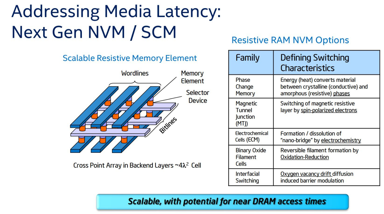
Intel presented an interesting slide during a recent presentation, listing all of the possible technologies based upon resistance change, and it listed PCM at the top. Although we are confident that 3D XPoint is PCM, or some variant thereof, some of these other technologies may be potential contenders.
Guy Blalock, the co-CEO of IMFT (from the Micron side), narrowed it down when he commented earlier this year at an event hosted by the SEMI trade group that 3D XPoint uses a chalcogenide material and an Ovonyx switch. Intel had a joint venture with Ovonyx and has licensed its technology in the past, but Micron purchased the firm for $1.3 billion in 2012 from Energy Conversion Devices (ECD). Ovonyx specializes in proprietary PCM technology (Phase-Change Memory).
Article continues belowPCM uses a chalcogenide glass-like material that takes advantage of voltage to create enough heat to change it between amorphous (high resistance) and crystalline (low resistance) states. The resulting change in electrical resistance signals a "1" for the crystalline state, or "0" for the amorphous state. There are also intermediary states between the absolute "1" and "0" settings, which allows for multiple bits per cell.
IMFT acknowledges that, for now, 3D XPoint only stores a single bit per cell (SLC), but that it can increase the bit count in future generations. Interestingly, IBM has already demonstrated three-bit-per-cell (TLC) PCM. It took nearly 10 years of mass SSD availability before the industry moved to storing multiple bits per NAND cell (MLC), so we could see a similarly slow trajectory with 3D XPoint. We are told that the company expects an 18-24 month cadence for newer generations of production-quality 3D XPoint, and MLC likely wouldn't happen within the first few generations.
Swabbing The Deck
The final material will consist of two layers, which Micron refers to as "decks," although at the time of the Flash Memory Summit in August 2016 IMFT was still working with prototype single-deck materials. There were newer 3D XPoint revisions arriving every 60-90 days, so Micron employed daughtercards on its SSD prototype (next page) that allow it to fast swap new revisions. The material will expand to a second deck when it has matured; perhaps it already has. The addition of a second deck does not increase speed by much, but it expands capacity. All of Micron's (and probably Intel's) performance demos were conducted with single deck prototypes.
There are numerous paths to increase density. Adding more bits per cell and shrinking the existing 20nm lithography (horizontal scaling) are obvious moves, along with adding more "decks," similar to how NAND is stacked into layers (vertical scaling). Notably, Intel indicates that decks are added in groups of two. Every two-deck addition doubles the capacity.
Get Tom's Hardware's best news and in-depth reviews, straight to your inbox.
IMFT manufactures 3D XPoint with a 20nm process that features a 128Gbit (16GB) die density (or 128 billion memory cells per chip), which is much lower than today's leading 64GB-per-die NAND. However, it is denser than DRAM, and IMFT can stack the die into packages, much like today's NAND. Micron is going to offer initial products with 1, 2, 4, and 8-die stacks. A 16-die stack could provide up to 256GB per package, but it is unclear if the company would stack the expensive die that high, because it could affect yields.
NAND can use TSV technology, which increases performance and reduces power consumption, but it remains to be seen if IMFT will employ it with 3D XPoint, which currently uses standard wire bonding. It would make sense to transition to TSV because it would unlock more of the potential performance of the underlying media.
3D All The Things
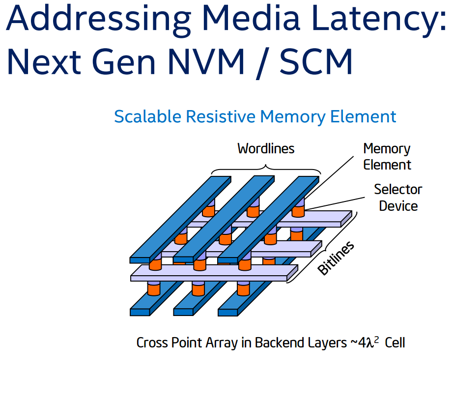
IMFT arranged the material in a crosspoint architecture, which is a common alignment for memory, denoting a chessboard-style series of bitlines and wordlines. There are many different uses for crosspoint architecture, so IMFT merely added some marketing magic to an established architecture naming convention to come up with its 3D XPoint moniker.
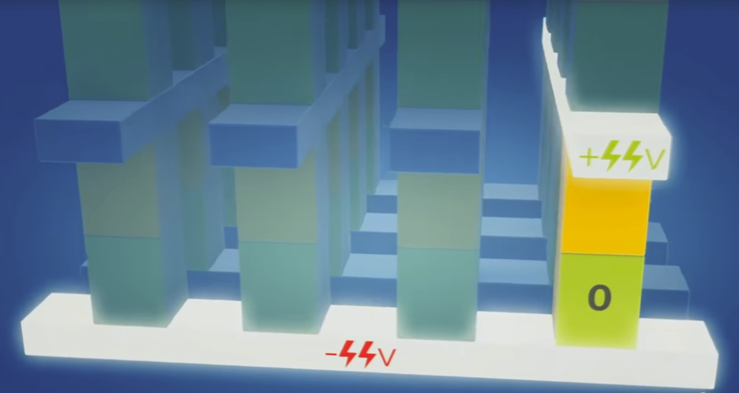
IMFT aligns the material into vertical columns, and each column has a memory cell (green) and a selector (yellow). The selector is an Ovonic Threshold Switch (OVS), which is a two-terminal device that consists of chalcogenide-based materials.
A series of perpendicular wires aligned into a 3D mesh connect the columns. The voltage flows through the wordline (top white bar; bitline is the bottom white bar) and into the selector, which then imparts a bulk material property change of the entire memory cell to write a binary value. Reading the memory cell requires a measurement of the resistance, which changes depending upon the state of the material. The controller accesses different cells by selecting different bitline/wordline combinations.
Micron indicates that the real innovation is in the selector, as opposed to the memory cell. In its simplest form, the selector is a diode. The design is easier to scale than transistor-based memories because transistors are hard to stack vertically. Existing memories are also electron-based and work by trapping electrons in insulators (and other electron trapping techniques), and the continued lithography shrinks result in fewer electrons per cell with each iterative generation. Current 2D NAND is already below a dozen electrons per cell, and even 3D NAND will encounter scaling limitations as lithographies shrink. Intel notes that while charge-based media isn't as scalable, resistance-based techniques enhance both scalability and performance.
Media Management
3D XPoint has a minimum erasable and writable unit of 1 bit, whereas NAND can write on the page level (16KB for Micron 3D NAND), but has to erase in much larger blocks (24MB). SSDs erase NAND cells before it reprograms them, so the SSD controller has to conduct garbage collection operations to ensure that the media has spare blocks available for the next round of incoming write data. The erase process invokes the tortuous endurance and performance killing read-modify-write cycle.
3D XPoint is a "write-in-place" memory. The SSD doesn’t have to erase existing data in the cells before it writes to them, so it overwrites it with a forced write process. As such, 3D XPoint endurance isn't measured in the normal program/erase cycles we are accustomed to with NAND-based SSDs; instead, its endurance is measured by the number of forced writes. The elimination of the erase cycle increases performance, simplifies management, and reduces wear.
3D XPoint's bit-addressable capability means that most of the old NAND rules no longer apply, or at least they don't have to. Even though 3D XPoint is bit addressable, Micron is using storage semantics with the QuantX line. The SSD versions overwrite to areas that are less than 512 bytes, which is far less than 24MB. This greatly reduces the need for data shuffling (which leads to write amplification) and lessens the impact of garbage collection, which helps with overall device performance and endurance.
Vendors normally fab NAND with a default 7% raw overprovisioning (OP), and then add more to meet certain endurance and performance profiles (the Effective OP). For instance, a low-capacity enterprise SSD usually has 30%-60% effective OP. 3D XPoint does not have any built-in raw overprovisioning, and the end product will have much less effective OP (30%-40% for all capacities). Extra OP for NAND-based SSDs serves to increase performance and endurance, but 3D XPoint will not require OP for speed; in contrast, the SSD will likely use it only to increase endurance.
NAND suffers from cell-to-cell interference due to electrons in neighboring cells. Other phenomena, such as read disturb, create wear just by reading data from adjacent cells. The resistance-based method, which doesn't use the electrons that serve as the catalyst for such issues, likely does not suffer these same peculiarities. However, there are inevitably other new media management challenges that we will learn about when 3D XPoint comes to market. The increased endurance also means that there is less focus on wear leveling, which helps to reduce overhead.
Unleashing Performance
3D XPoint's die design is one of the keys to its speed. Manufacturers separate NAND die into multiple planes per die, and each plane can respond independently to incoming program/erase commands. More planes per die extract more parallelism, and thus performance, from a single die. Micron's own 3D NAND holds the record for the most planes on a single modern NAND die, at four. Vendors do not increase the number of planes per die because it decreases density, which increases cost.
Micron revealed that although it doesn't split the 3D XPoint die into what would we consider normal planes, it does have 64 regions that respond independently to program/erase commands (analogous to a 64-plane architecture). The design means that each 3D XPoint die can respond to requests like a 16 quad-plane NAND die, which is probably one of the reasons it offers such tremendous performance under heavy load. The increased performance at low queue depths is a result of the media being faster. It responds to commands almost immediately.
Current page: Just What Is 3D XPoint?
Prev Page The IMFT Sideshow Next Page Endurance, Power, And Materials
Paul Alcorn is the Editor-in-Chief for Tom's Hardware US. He also writes news and reviews on CPUs, storage, and enterprise hardware.
-
coolitic the 3 months for data center and 1 year for consumer nand is an old statistic, and even then it's supposed to apply to drives that have surpassed their endurance rating.Reply -
Paul Alcorn Reply18916331 said:the 3 months for data center and 1 year for consumer nand is an old statistic, and even then it's supposed to apply to drives that have surpassed their endurance rating.
Yes, that is data retention after the endurance rating is expired, and it is also contingent upon the temperature that the SSD was used at, and the temp during the power-off storage window (40C enterprise, 30C Client). These are the basic rules by which retention is measured (the definition of SSD data retention, as it were), but admittedly, most readers will not know the nitty gritty details.
However, I was unaware that JEDEC specification for data retention has changed, do you have a source for the new JEDEC specification?
-
stairmand Replacing RAM with a permanent storage would simply revolutionise computing. No more loading an OS, no more booting, no loading data, instant searches of your entire PC for any type of data, no paging. Could easily be the biggest advance in 30 years.Reply -
InvalidError Reply
You don't need X-point to do that: since Windows 95 and ATX, you can simply put your PC in Standby. I haven't had to reboot my PC more often than every couple of months for updates in ~20 years.18917236 said:Replacing RAM with a permanent storage would simply revolutionise computing. No more loading an OS, no more booting, no loading data
-
Kewlx25 Reply18918642 said:
You don't need X-point to do that: since Windows 95 and ATX, you can simply put your PC in Standby. I haven't had to reboot my PC more often than every couple of months for updates in ~20 years.18917236 said:Replacing RAM with a permanent storage would simply revolutionise computing. No more loading an OS, no more booting, no loading data
Remove your harddrive and let me know how that goes. The notion of "loading" is a concept of reading from your HD into your memory and initializing a program. So goodbye to all forms of "loading". -
hannibal The Main thing with this technology is that we can not afford it, untill Many years has passesd from the time it comes to market. But, yes, interesting product that can change Many things.Reply -
TerryLaze Reply
Sure you won't be able to afford a 3Tb+ drive in even 10 years,but a 128/256Gb one just for windows and a few games will be affordable if expensive even in a couple of years.18922543 said:10 years later... still unavailable/costs 10k
-
zodiacfml I dont understand the need to make it work as DRAM replaement. It doesnt have to. A system might only need a small amount RAm then a large 3D xpoint pool.Reply
The bottleneck is thr interface. There is no faster interface available except DIMM. We use the DIMM interface but make it appear as storage to the OS. Simple.
It will require a new chipset and board though where Intel has the control. We should see two DIMM groups next to each other, they differ mechanically but the same pin count.


