3D XPoint: A Guide To The Future Of Storage-Class Memory
Memory and storage collide with Intel and Micron's new, much-anticipated 3D XPoint technology, but the road has been long and winding. This is a comprehensive guide to its history, its performance, its promise and hype, its future, and its competition.
Get Tom's Hardware's best news and in-depth reviews, straight to your inbox.
You are now subscribed
Your newsletter sign-up was successful
The Economics And Competition
The first true hurdle for any semiconductor product is the economics of bringing it to market. 3D XPoint uses over 100 new materials, and (we assume) a new production flow. We do know that the fab tooling is new and requires significant expenditures, which means that the technology can't piggyback off some of the learning, processes, and tooling of previous generations, like NAND and DRAM do.
Ultimately, production scale lowers cost, but to build scale you need a low cost. Intel and Micron find themselves in this classic chicken-and-egg scenario. Micron has been quite vocal that it doesn't expect to make any money the first few years as it (rightly) focuses on building the ecosystem and production scale, and Intel is in the same boat.
As usual, scale should come in the client market, but profit will flow from the lucrative enterprise segment. NAND vendors help build scale by shipping it en masse into client use-cases for low-end applications, such as USB sticks. That won't be a viable method to build scale for 3D XPoint, but the client market will likely be a key portion of Intel's strategy.
Article continues below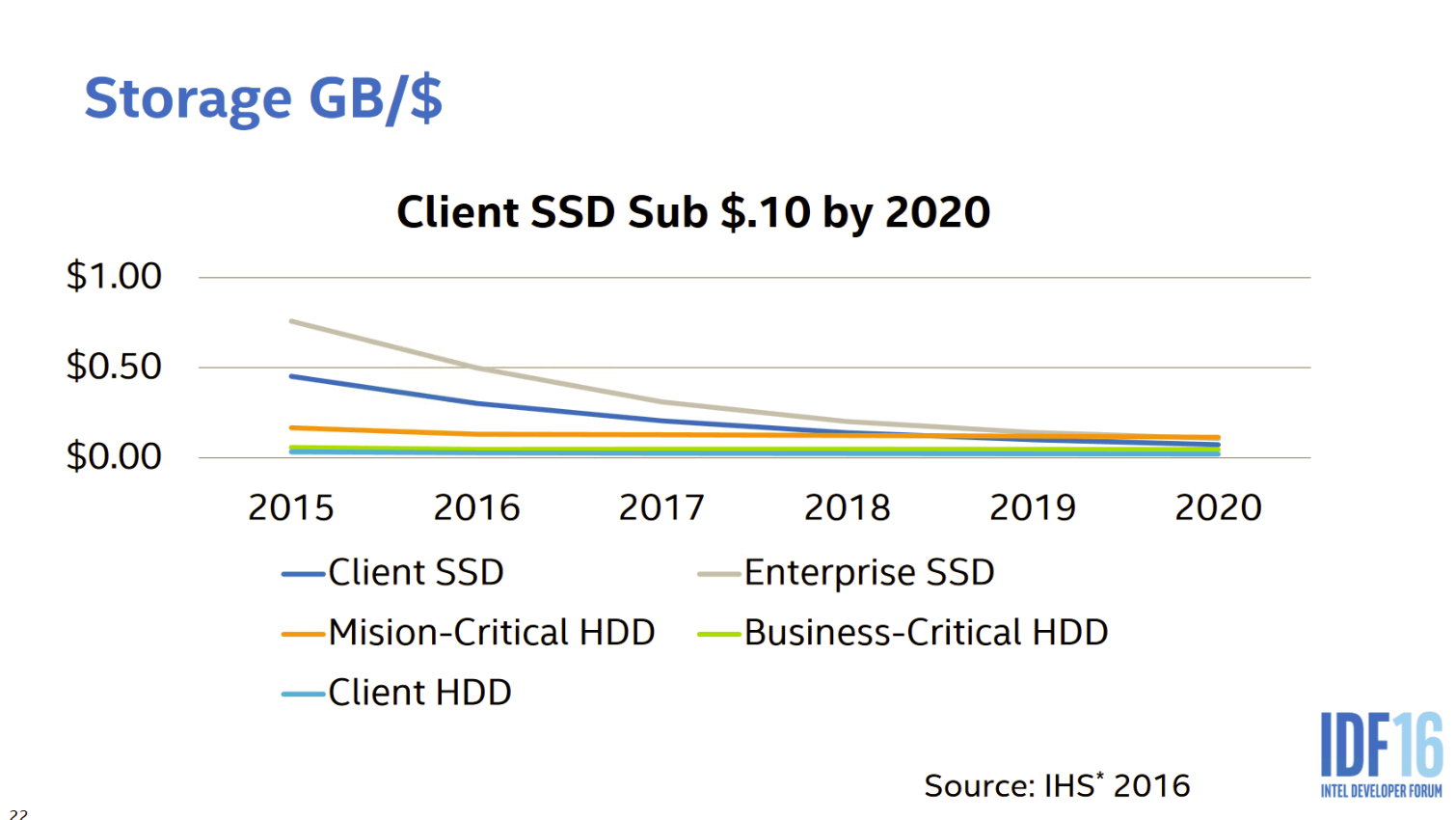
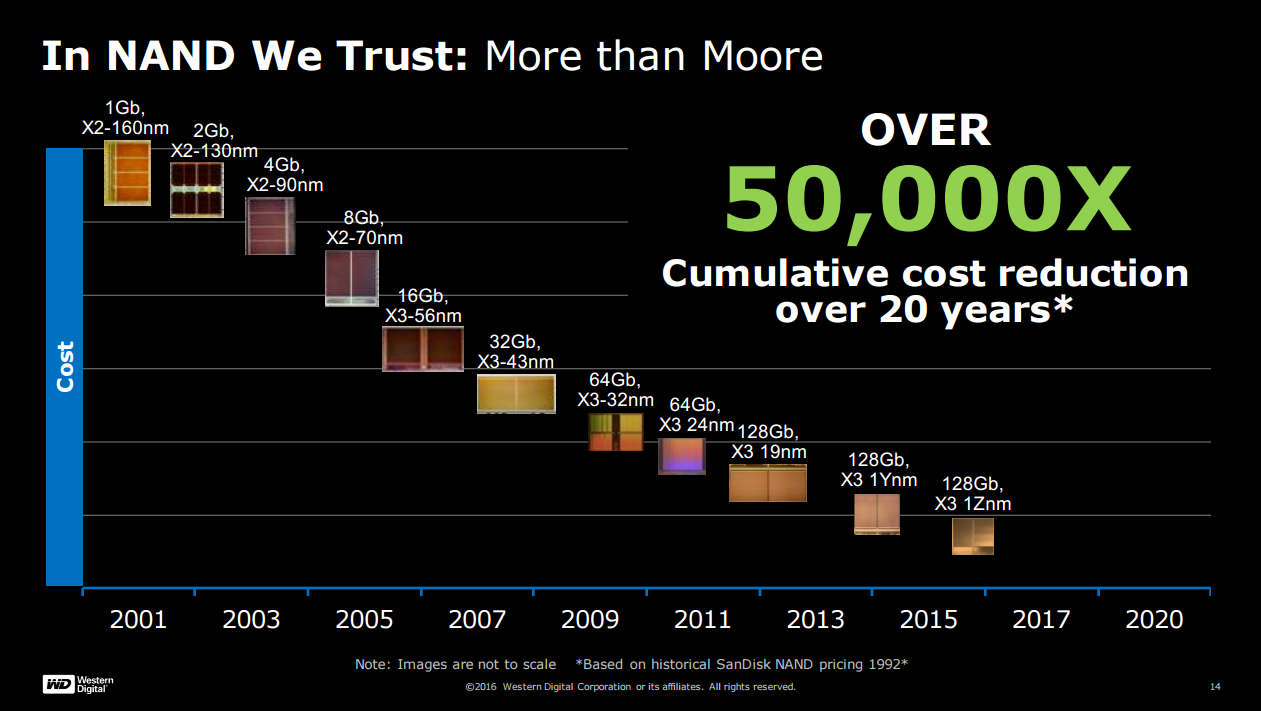
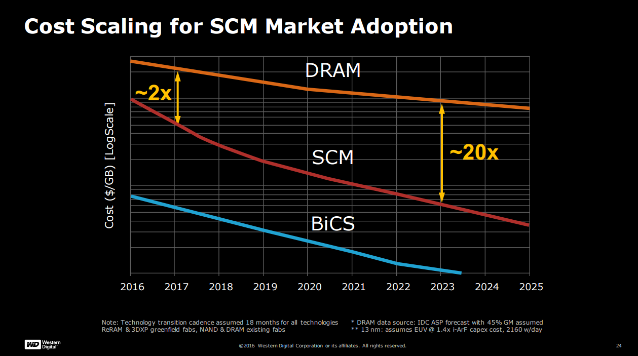

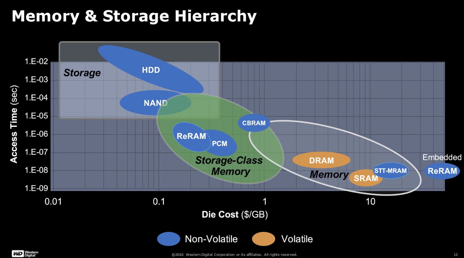
NAND required 20 years to experience broad adoption, and that has come largely on the back of a 50,000X price decrease over that time. Intel's projections have NAND pricing falling below $0.10 per GB by 2020. New use cases for employing NAND as memory are already proliferating, and the low price means NAND could actually compete and slow 3D XPoint adoption. WD doesn't feel that any competing tech will be cheap enough, which the company surmises needs to be in the range of 20X less expensive than DRAM, until the 2020 time frame. The lack of production scale and the breathtaking capital expenditures associated with building it are the primary culprit. For instance, a greenfield 3D NAND fab weighs in at roughly $8 billion, and that is with a proven and mature technology with standard tooling.
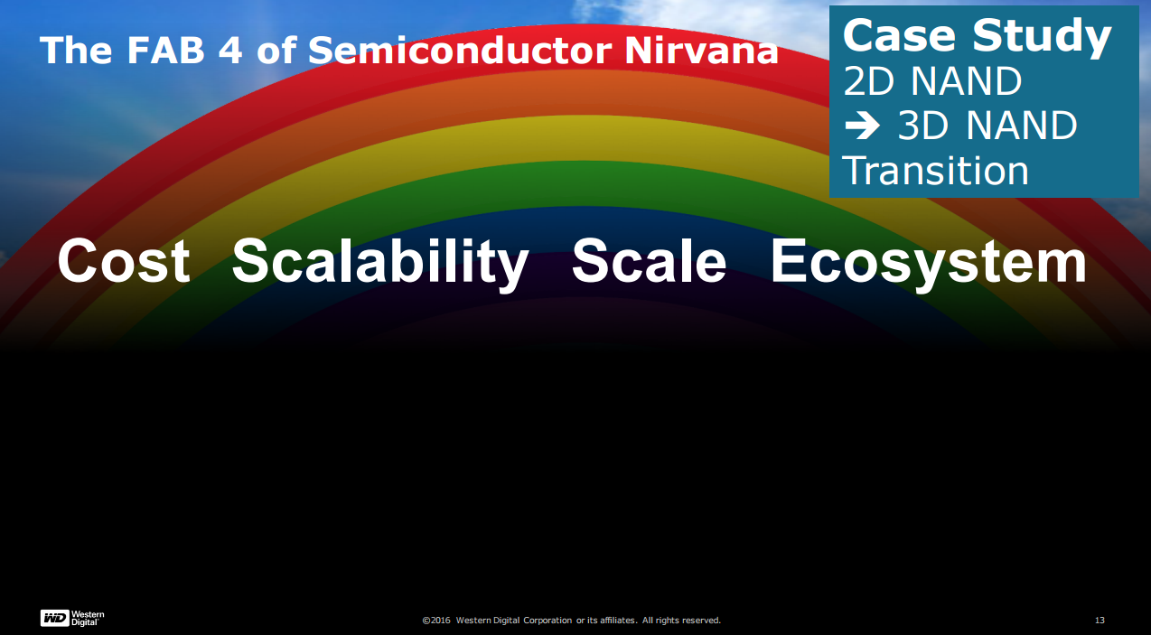
To highlight its NAND production scale, WD noted that if it stacked all of the wafers (horizontally, mind you) that it produces at just one fab in a year, it would be taller than Mount Kilimanjaro. While the output is surprising, it shouldn't be; WD's Shanghai facility punches out two million flash devices per day. This doesn't account for WD's other fabs, or the rest of the industry's production. It is highly unlikely that 3D XPoint will attain this level of scale in the near future, and because production is limited to IMFT, it might relegate it to the high end of the price spectrum for quite some time.
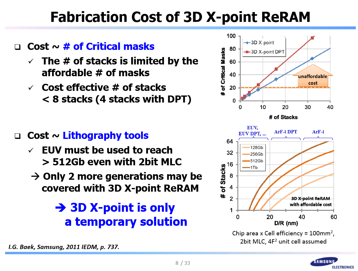
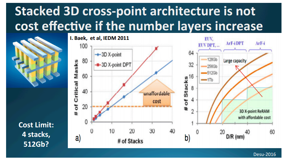
The final two slides originate from a Samsung whitepaper presented in 2012, which contends that 3D crosspoint architectures are not scalable in a cost-effective manner over the long term. The lithography tools and the need for EUV for advanced nodes (which IMFT has acknowledged for 3D XPoint) are significant barriers, along with the number of lithography steps. It's noteworthy that SanDisk has also expressed a similar opinion that 3D crosspoint architectures aren't scalable--and it speaks from experience, since it has shipped multi-layer crosspoint architectures in volume in the past.
IMFT may have the silver bullet to solve the production challenges, but it’s apparent that other industry heavyweights are skeptical.
Get Tom's Hardware's best news and in-depth reviews, straight to your inbox.
The Competition
There are several new types of memory jockeying for a position in the new world of persistent memories, and the industry has broadly begun to refer to this collective group as Storage Class Memory (SCM). Of course, everyone wants a piece of the pie, and numerous industry stalwarts have their own independent plans.
A blizzard of acronyms greets anyone who wishes to forge into the future memory landscape, but each has its own weaknesses and advantages. The contenders include ReRAM, STT-RAM, PCM, Memristors, MRAM, CBRAM, NRAM, and FeRAM, among others. The goal is mostly the same: address the gap between storage and memory with a persistent memory.
| Header Cell - Column 0 | Memristor | PCM | STT-RAM | ReRAM | DRAM | Flash | HDD |
|---|---|---|---|---|---|---|---|
| Read Time (ns) | <10 | 20-70 | 10-30 | 10 | 10-50 | 25,000 | 5-8x10⁶ |
| Write Time (ns) | 20-30 | 50-500 | 13-95 | 1-100 | 10-50 | 200,000 | 5-8x10⁶ |
| Endurance (cycles) | 1 Trillion | 10 - 100 million | 1015 | 1010-1012 | >1017 | 500-106 | 1015 |
| Retention (without power) | >10 Years | <10 Years | Weeks | Months | <Second | ~10 Years | ~10 Years |
| Energy Per Bit (pj)2 | 0.1-3 | 2-100 | 0.1-1 | ? | 2-4 | 101-1014 | 106-107 |
| Chip Area Per Bit (F2) | 4 | 8-16 | 14-64 | ? | 6-8 | 4-8 | n/a |
Of course, we don't have enough information to include 3D XPoint in the chart above, but it does give us a good indication of the current layout of the market and the relative competitiveness of each medium. If you believe the industry sentiment, and the IMFT CEO's faux pas, then you have to look no further than the PCM column to see what the base 3D XPoint material is capable of.
Samsung presents a clear threat with existing technology that performs well at a huge price advantage. WD and Toshiba will produce 3D ReRAM, but have no plans to begin production until at least 2020. Micron's own "EM Gen 1" will purportedly be a faster than 3D XPoint and the company will begin production in 2017. There is no indication that Intel is involved in its development.
Current page: The Economics And Competition
Prev Page Storage Or Memory, Or Both? Next Page Where To Go From Here
Paul Alcorn is the Editor-in-Chief for Tom's Hardware US. He also writes news and reviews on CPUs, storage, and enterprise hardware.
-
coolitic the 3 months for data center and 1 year for consumer nand is an old statistic, and even then it's supposed to apply to drives that have surpassed their endurance rating.Reply -
Paul Alcorn Reply18916331 said:the 3 months for data center and 1 year for consumer nand is an old statistic, and even then it's supposed to apply to drives that have surpassed their endurance rating.
Yes, that is data retention after the endurance rating is expired, and it is also contingent upon the temperature that the SSD was used at, and the temp during the power-off storage window (40C enterprise, 30C Client). These are the basic rules by which retention is measured (the definition of SSD data retention, as it were), but admittedly, most readers will not know the nitty gritty details.
However, I was unaware that JEDEC specification for data retention has changed, do you have a source for the new JEDEC specification?
-
stairmand Replacing RAM with a permanent storage would simply revolutionise computing. No more loading an OS, no more booting, no loading data, instant searches of your entire PC for any type of data, no paging. Could easily be the biggest advance in 30 years.Reply -
InvalidError Reply
You don't need X-point to do that: since Windows 95 and ATX, you can simply put your PC in Standby. I haven't had to reboot my PC more often than every couple of months for updates in ~20 years.18917236 said:Replacing RAM with a permanent storage would simply revolutionise computing. No more loading an OS, no more booting, no loading data
-
Kewlx25 Reply18918642 said:
You don't need X-point to do that: since Windows 95 and ATX, you can simply put your PC in Standby. I haven't had to reboot my PC more often than every couple of months for updates in ~20 years.18917236 said:Replacing RAM with a permanent storage would simply revolutionise computing. No more loading an OS, no more booting, no loading data
Remove your harddrive and let me know how that goes. The notion of "loading" is a concept of reading from your HD into your memory and initializing a program. So goodbye to all forms of "loading". -
hannibal The Main thing with this technology is that we can not afford it, untill Many years has passesd from the time it comes to market. But, yes, interesting product that can change Many things.Reply -
TerryLaze Reply
Sure you won't be able to afford a 3Tb+ drive in even 10 years,but a 128/256Gb one just for windows and a few games will be affordable if expensive even in a couple of years.18922543 said:10 years later... still unavailable/costs 10k
-
zodiacfml I dont understand the need to make it work as DRAM replaement. It doesnt have to. A system might only need a small amount RAm then a large 3D xpoint pool.Reply
The bottleneck is thr interface. There is no faster interface available except DIMM. We use the DIMM interface but make it appear as storage to the OS. Simple.
It will require a new chipset and board though where Intel has the control. We should see two DIMM groups next to each other, they differ mechanically but the same pin count.
