AMD A10-7850K And A8-7600: Kaveri Gives Us A Taste Of HSA
We've spent the days following CES benchmarking two of AMD's new Kaveri-based APUs. Do the Steamroller x86 architecture, GCN graphics design, and HSA-oriented features impress, or do they come up short against Intel's value-oriented Haswell-based parts?

Steamroller, GCN, HSA, 28 nm: Oh My!
This year’s CES was my most insane to date. I showed up in Vegas two days earlier, stayed a day later, and managed to fit close to 50 different meetings into a schedule that started early in the morning and didn’t end until late at night. But by the end, I had a solid grasp on the technologies we’ll be seeing in 2014. Some of them are decidedly evolutionary. Others, like Oculus’ Crystal Cove prototype, will fundamentally change PC gaming for the better.
For AMD’s part, it spent CES talking about Kaveri—a design that, on paper, should be interesting stuff for enthusiasts. There are the Steamroller-based x86 cores, giving us a new processor architecture to talk about. This is also the first time AMD’s vaunted Graphics Core Next design finds its way into an APU. The company did a ton of work enabling Heterogeneous System Architecture features for better interplay between computing resources and software developers. And it’s using a new 28 nm manufacturing process from GlobalFoundries.
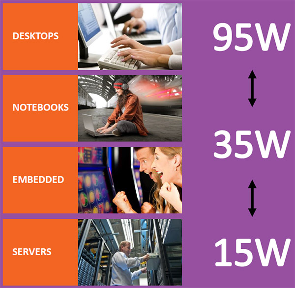
But although this week's introduction focused on the top-end 95 W A10-7850K, the real emphasis of Kaveri is down in the lower-power segments. Company representatives say engineers designed for the 35 to 45 W range, scaling as high as 95 and as low as 15 W. AMD wants to see APUs in desktops, notebooks, embedded environments, and servers. So, it took the middle road in order to better optimize for those targets. AMD also had to make some compromises on the manufacturing side, better balancing transistor density to enable a 512-shader Radeon graphics core, while ultimately sacrificing CPU speed.
Article continues belowOf course, at the end of the day, once we’ve carefully carved through the architecture and AMD’s vision for Kaveri, what matters most is how this APU family compares to what came before and Intel’s best effort in the same space.
Building A Better Computing Device
Integration is a word that gets thrown around a lot, and often with negative connotation. Ew, integrated graphics, right? But integration is an important part of making complex technologies more affordable. In many cases, it’s very, very good for performance. And there's typically a positive correlation with power, too. By now we all know that AMD’s APUs combine multiple subsystems to allow the fast movement of data between programmable and fixed-function logic, maximizing flexibility and, ideally, making it possible to run demanding workloads on affordable hardware.
That Kaveri includes multiple x86 cores, graphics processing, memory control, cache, hardware-based accelerators, and PCI Express connectivity on a single piece of silicon is no surprise; its predecessor offered a similarly-thorough list of capabilities as well. But if you think of Kaveri as a puzzle, AMD took each piece and tweaked it in such a way that the finished product would reflect the latest technologies, more advanced manufacturing, and another step toward the company’s vision of utilizing the most appropriate resources for any workload.
One component of this approach involved re-thinking lithography. In partnership with GlobalFoundries, AMD is shifting from 32 nm SOI to a 28 nm bulk silicon process. Now, there are associated advantages and disadvantages. Previously, AMD was building its APUs using technology optimized for CPUs. That allowed chips like the A10-6800K to hit clock rates as high as 4.4 GHz through Turbo Core. But tuning for low density, low resistance, and ultimately higher frequencies negatively affected the number of transistors that AMD could fit on a die, limiting the complexity of its GPU. In a world where x86 cores are considered “fast enough” in workloads that wait for user input, the decision was made to slide the scale toward density. AMD calls this APU-optimized, but the bottom line is that it’s using slower, higher-resistance transistors in order to facilitate better area utilization.
Get Tom's Hardware's best news and in-depth reviews, straight to your inbox.
The consequence is lower-frequency x86 cores, which you’ll see reflected in a comparison of Kaveri and Richland. AMD says it compensates with a transition from the Piledriver architecture to Steamroller. A focus on improving IPC—or the amount of work each core does per cycle—purportedly yields up to 20% gains, leaving Kaveri net-positive in most x86 workloads.
On the other hand, the APU sports a more potent graphics subsystem, wielding up to 512 shaders based on the GCN architecture. Richland topped out at 384 of the previous-gen VLIW4 ALUs. This clear re-distribution of transistor wealth in favor of the GPU better-addresses the performance-sensitive workloads AMD is targeting (gaming, multimedia, and content creation), while maintaining a status quo in more general-purpose tasks.
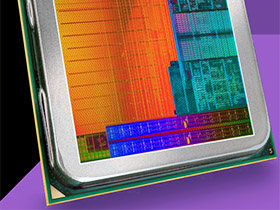
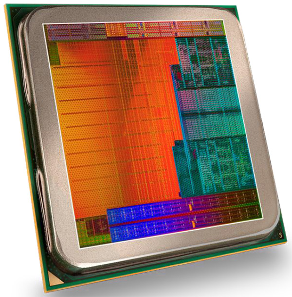
All told, Kaveri is a 2.41 billion-transistor SoC crammed into 245 square millimeters. Richland was nearly the same size (246 mm²), but comprising just 1.3 billion transistors. Do you like that? We’re now dismissing billion-plus-transistor processors as pedestrian. This all goes to show the impact of AMD’s shift to 28 nm bulk silicon, optimized for a more GPU-focused die, though.
The Kaveri Family, As It Exists Today
Two models (A10-7850K and A10-7700K) are expected to ship immediately, with a third (A8-7600) surfacing in the first quarter of 2014. The flagship is priced at $173. So, you get a lot of additional goodness, but pay an additional 22% compared to A10-6800K. Even the -7700K is pricier than last-gen's fastest offering at $152. Ahead of its official debut, the -7600 is expected to sell for $119.
| Header Cell - Column 0 | A10-7850K | A10-7700K | A8-7600 |
|---|---|---|---|
| Graphics Level | Radeon R7 | Radeon R7 | Radeon R7 |
| TDP | 95 W | 95 W | 65/45 W |
| CPU Cores | 4 | 4 | 4 |
| CPU Base Clock Rate | 3.7 GHz | 3.4 GHz | 3.3 / 3.1 GHz |
| Max. Turbo Core Clock Rate | 4 GHz | 3.8 GHz | 3.8 / 3.3 GHz |
| GPU Shaders | 512 | 384 | 384 |
| GPU Clock Rate | 720 MHz | 720 MHz | 720 MHz |
| "Compute Cores" | 12 | 10 | 10 |
| Price | $173 | $152 | $119 |
Both of the just-launched Kaveri-based APUs are 95 W parts (ironically, the thermal ceiling AMD appears least concerned with).
A10-7850K sports two Steamroller modules and 512 shaders. The processor’s base clock rate is 3.7 GHz, though it can reach up to 4 GHz in lightly threaded apps. Meanwhile, the R7 graphics engine operates at 720 MHz.
In fact, all three Kaveri models sport GPUs at 720 MHz. The biggest difference between A10-7850K and the other two SKUs is shader count. A10-7700K and A8-7600 both come with 384. The -7700 operates at a 3.4 GHz base clock that ramps up as high as 3.8 GHz under the right thermal conditions.
The A8-7600 is unique in that it offers a TDP that can be manually configured to 65 or 45 W. A higher thermal ceiling allows for a 3.3 GHz base clock and 3.8 GHz peak, while the 45 W setting keeps the APU cycling between 3.1 and 3.3 GHz.
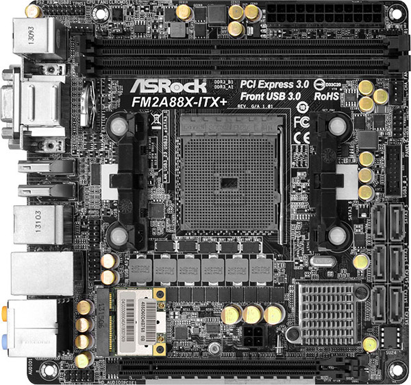
Kaveri-based APUs drop into a new interface called Socket FM2+. We’ve already seen compatible motherboards employing AMD’s A88X, A78, A75, and A55 Fusion Controller Hubs; it’s really up to each board vendor to hit the right price points with Socket FM2+. You can use Socket FM2-based APUs on FM2+-equipped boards, but not vice versa. A block diagram of the Kaveri die also reveals a PCI Express 3.0 controller (presumably with 16 lanes of connectivity, given the motherboards we have in the lab so far), support for up to four display outputs, and the same XDMA engines found in AMD’s Hawaii GPU for CrossFire (in this case, enabling Dual Graphics functionality). We’ll go into multi-GPU rendering in greater depth later in today’s story.
Current page: Steamroller, GCN, HSA, 28 nm: Oh My!
Next Page Meet The Compute Core-
Someone Somewhere Yeah, almost all the diagrams refer to the 4760K.Reply
Given that AM3+ looks like it's done, it would have been nice to see a 6-core chip. Still, one of these may end up in my next laptop. -
spp85 A10-7850k is slower than A10-6800K ?? WTF. Its all hype than actual performance to the table. Even on OpenCL GPU accelerated apps doesn't have any advantage with A10-7850k over i5 or sometimes i3 CPUs. Hopeless is what I feel about AMD CPUs.Reply -
Someone Somewhere Reply12454254 said:A10-7850k is slower than A10-6800K ?? WTF.
I got the opposite impression. Which graph are you looking at? -
Jaroslav Jandek Thank you for the article (especially the power consumption measurements), Chris. It is definitely an improvement over Richland but kind of boring (disappointingly expectable).Reply
I really like where AMD is going (HSA, GCN and TrueAudio).Too bad the manufacturing process of GlobalFoundries just can't match Intel's.
Also, it would be interesting to see the new Bay Trail Pentium or Celeron CPUs (whichever is closer in performance) in the Efficiency graphs. -
Someone Somewhere I'm fairly sure that this is on TSMC's 28nm node. GlobalFoundries can't do that yet; this is on the same process used for AMD GPUs currently.Reply -
Jaroslav Jandek Reply
28nm SHP from GlobalFoundries. AMD bought over $1 billion worth of wafers from them in december...12454280 said:I'm fairly sure that this is on TSMC's 28nm node. GlobalFoundries can't do that yet; this is on the same process used for AMD GPUs currently.
I guess you have been reading the articles from a year ago about AMD still using TSMC despite promises of GlobalFoundries' new 28nm SHP process. -
jacobian I don't really believe into the whole HSA smoke-screen. By the time HSA-enabled apps take off, you will be ready to upgrade from your CPU again. The one terrible truth that stands out right now is that at current prices, the flagship Kaveri A10 doesn't make any sense whatsoever. Kaveri A8? Maybe. Richland A10-6790K? Perhaps. But the Kaveri A10 at $180 is a just a joke, specially after all that hype.Reply -
Someone Somewhere CPUs are usually released at ridiculous prices, and come down over a month or two.Reply


