AMD A10-7850K And A8-7600: Kaveri Gives Us A Taste Of HSA
We've spent the days following CES benchmarking two of AMD's new Kaveri-based APUs. Do the Steamroller x86 architecture, GCN graphics design, and HSA-oriented features impress, or do they come up short against Intel's value-oriented Haswell-based parts?
A More Capable GPU: GCN Surfaces In Kaveri
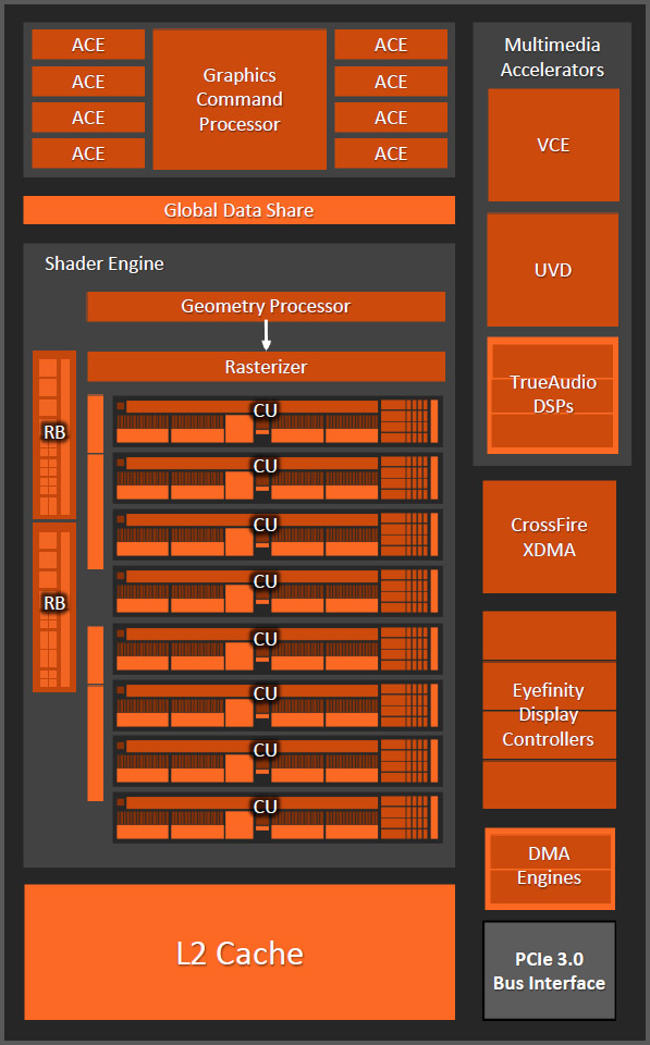
I’m a bit of geek in that I get excited about testing the differences between subsequent processor designs. But Steamroller really only serves as an enabler for AMD’s Graphics Core Next architecture in Kaveri, improving IPC enough so that the more dense APU doesn’t sacrifice too much general-purpose performance as the graphics subsystem grows. In fact, AMD says Kaveri’s GPU accounts for 47% of the die.
The engine is composed of up to eight GPU “cores”, formerly referred to as Compute Units, and made up of four Vector Units with 16 shaders each. In total, that’s 64 shaders per core and 512 shaders in an eight-core implementation. Don’t let the numbers or evolving terminology confuse you though. Architecturally, this is the same technology found in AMD’s Hawaii GPU, which I covered in Radeon R9 290X Review: AMD's Back In Ultra-High-End Gaming, including precision improvements to the native LOG/EXP operations and MQSAD optimizations for speeding up motion estimation algorithms, mentioned back when Hawaii launched. Of course, the big addition is coherent shared unified memory. That coherency makes it easier to pass data between the GPU and CPU cores—again, the degree of “equalness” between dissimilar on-die resources is the exact reason why AMD is using the term Compute Core to begin with.
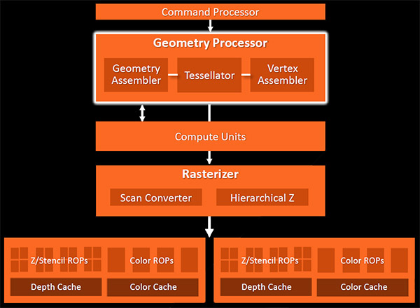
There’s a lot of strategic trimming that goes into optimizing Kaveri’s GPU compared to AMD’s discrete solutions. The Hawaii GPU has four geometry processors able to rasterize as many primitives per clock cycle. Tahiti features two. Kaveri gets one. And while 16 render back-ends give Hawaii massive pixel fillrate, Kaveri is pared down to two ROP partitions, capable of eight pixels per clock. Given the bandwidth limitations of an integrated solution attached to DDR3 memory, those design decisions make perfect sense.
Not every piece of the Kaveri GPU is a subset of Hawaii. AMD exposes all eight of the discrete processor’s Asynchronous Compute Engines, which independently schedule tasks to the CUs (incidentally, Sony’s PlayStation 4 also boasts eight ACEs). They all share access to a global data share and a 512 KB L2 cache. But they can otherwise operate on their own for efficient multi-tasking. Back when I was digging into Hawaii, the shift from two ACEs in Tahiti to four in Kabini/Temash and then eight didn’t seem imminently necessary. Now that we’re seeing the design exposed on Kaveri, however, its importance to AMD’s HSA is clearer.
Fixed-Function Accelerators: More Specialized Hardware
I already mentioned that Kaveri lacks fixed-function support for H.265 decoding. However, the old faithful Unified Video Decoder is in there, accelerating playback of H.264, VC-1, MPEG-2, MVC, and MPEG-4. In essence, the “new” UVD 4 in Kaveri is similar to the older UVD 3 block, except for improved error resiliency during AVC decoding.
AMD also claims to have improved its Video Codec Engine, adding I, P, and B frame support to the common H.264 YUV420 video format and I frames to the simpler YUV444 format. To be sure, we’re happy to see AMD adding to the VCE block’s functionality. However, our most recent look at the VCE’s performance put AMD behind Nvidia’s NVEnc solution and significantly slower than Intel’s Quick Sync. So, while Kaveri’s second-gen VCE might represent a functional step forward, we want to see more attention paid to its position relative to competitive encoders.
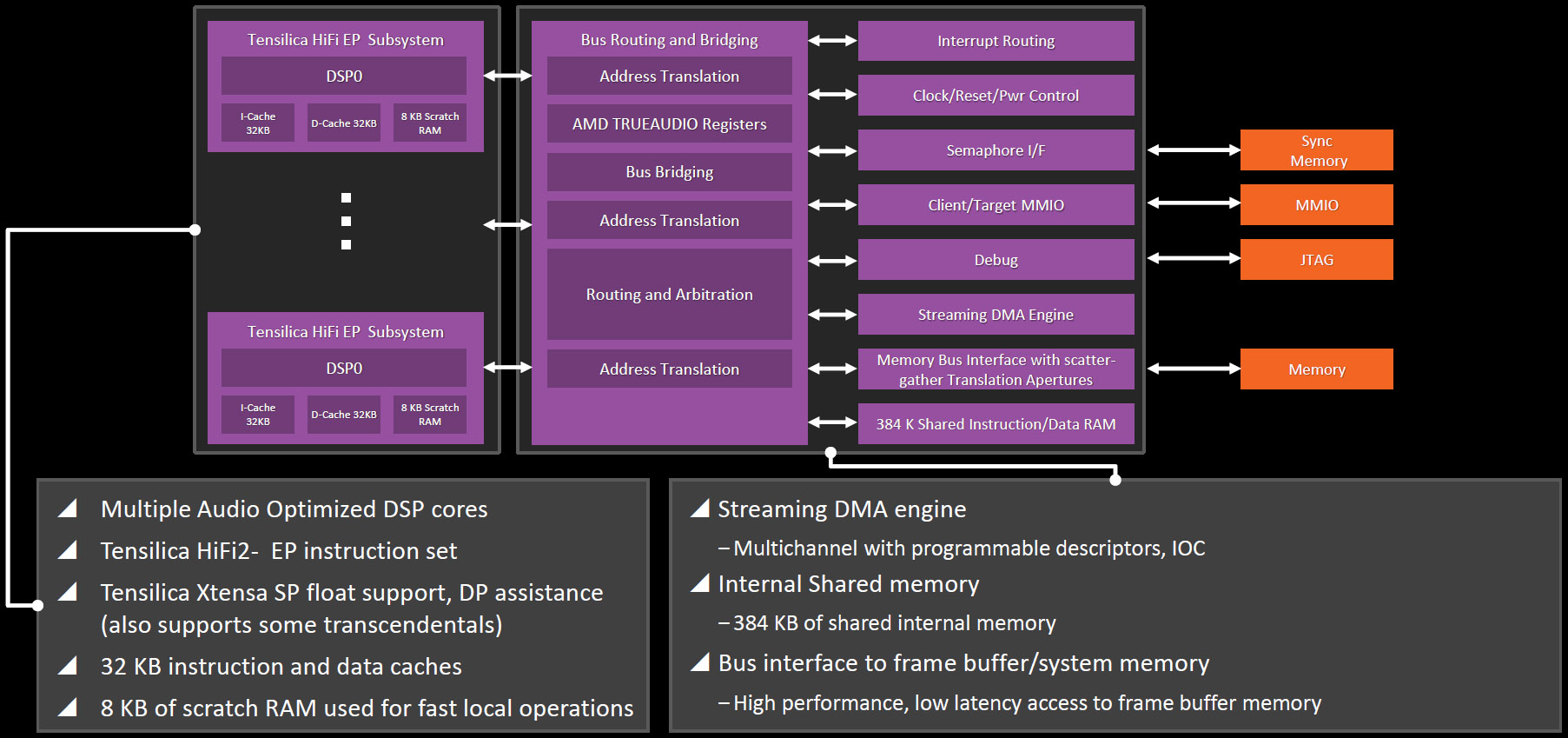
As with the Hawaii and Bonaire GPUs powering Radeon R9 290X, 290, and R7 260X, Kaveri includes TrueAudio support. That means there are, presumably, three Tensilica HiFi2 EP Audio DSP cores built into the APU’s die able to offload sound processing. I say Kaveri supports this technology because it needs to be exploited in software before you realize any benefit, and thus far there aren’t any applications we can use to illustrate TrueAudio’s impact. At least in practice, it’s intended to facilitate more complex effects without a corresponding drain on host resources. But every attempt we’ve seen to demonstrate TrueAudio hasn’t translated particularly well to a conference room setting.
Get Tom's Hardware's best news and in-depth reviews, straight to your inbox.
Current page: A More Capable GPU: GCN Surfaces In Kaveri
Prev Page Meet The Compute Core Next Page Enabling HSA On The Kaveri APU-
Someone Somewhere Yeah, almost all the diagrams refer to the 4760K.Reply
Given that AM3+ looks like it's done, it would have been nice to see a 6-core chip. Still, one of these may end up in my next laptop. -
spp85 A10-7850k is slower than A10-6800K ?? WTF. Its all hype than actual performance to the table. Even on OpenCL GPU accelerated apps doesn't have any advantage with A10-7850k over i5 or sometimes i3 CPUs. Hopeless is what I feel about AMD CPUs.Reply -
Someone Somewhere Reply12454254 said:A10-7850k is slower than A10-6800K ?? WTF.
I got the opposite impression. Which graph are you looking at? -
Jaroslav Jandek Thank you for the article (especially the power consumption measurements), Chris. It is definitely an improvement over Richland but kind of boring (disappointingly expectable).Reply
I really like where AMD is going (HSA, GCN and TrueAudio).Too bad the manufacturing process of GlobalFoundries just can't match Intel's.
Also, it would be interesting to see the new Bay Trail Pentium or Celeron CPUs (whichever is closer in performance) in the Efficiency graphs. -
Someone Somewhere I'm fairly sure that this is on TSMC's 28nm node. GlobalFoundries can't do that yet; this is on the same process used for AMD GPUs currently.Reply -
Jaroslav Jandek Reply
28nm SHP from GlobalFoundries. AMD bought over $1 billion worth of wafers from them in december...12454280 said:I'm fairly sure that this is on TSMC's 28nm node. GlobalFoundries can't do that yet; this is on the same process used for AMD GPUs currently.
I guess you have been reading the articles from a year ago about AMD still using TSMC despite promises of GlobalFoundries' new 28nm SHP process. -
jacobian I don't really believe into the whole HSA smoke-screen. By the time HSA-enabled apps take off, you will be ready to upgrade from your CPU again. The one terrible truth that stands out right now is that at current prices, the flagship Kaveri A10 doesn't make any sense whatsoever. Kaveri A8? Maybe. Richland A10-6790K? Perhaps. But the Kaveri A10 at $180 is a just a joke, specially after all that hype.Reply -
Someone Somewhere CPUs are usually released at ridiculous prices, and come down over a month or two.Reply


