Radeon R9 290X Review: AMD's Back In Ultra-High-End Gaming
After eight months of watching Nvidia go uncontested in the ultra-high-end graphics market, AMD has a new GPU based on existing technology that promises to challenge the top position. It gets mighty loud at times, but you can't ignore the R9 290X's price.
Hawaii: A 6.2 Billion Transistor GPU For Gaming
Today, the fastest single-GPU graphics card is Nvidia’s GeForce GTX Titan (Benchmarking GeForce GTX Titan 6 GB: Fast, Quiet, Consistent). It sells for no less than $1000 and comes equipped with 6 GB of fast GDDR5 memory. By all accounts, it’s really well-suited for gaming at 2560x1440, it serves up playable performance at 5760x1080 in some games, but doesn’t quite move fast enough for 3840x2160. In fact, in Gaming At 3840x2160: Is Your PC Ready For A 4K Display?, I came to the conclusion that it’d take a couple of GeForce GTX 780s to serve up satisfactory frame rates on an Ultra HD screen.
And now AMD is billing its new Radeon R9 290X as a ready-for-4K solution. Them’s fighting words, particularly with Ultra HD targeted as the next frontier in PC gaming. The technology is still very expensive, and it’s far from refined. But I challenge you to enjoy your favorite title on a 32”, 8.3-million-pixel screen, and then hand it back willingly. Expect 4K to be the battleground on which AMD and Nvidia drop their high-end GPUs moving forward.
Last week, while Nvidia put on an event in Montreal to announce a handful technologies and initiatives, including an upcoming GeForce GTX 780 Ti, AMD was taking the wraps off of a few benchmark results that indeed showed the 290X faster than GeForce GTX 780 in BioShock Infinite and Tomb Raider at 3840x2160.
What is at the heart of this new board, which seemed to effortlessly speed past Nvidia’s $650 solution? The Hawaii GPU—a much more complex piece of silicon than Tahiti, based on the same Graphics Core Next architecture. Think of it as a little bit of old and a little bit of new.
Is AMD Back To The "Big GPU" Approach?
All the way back in 2007, AMD altered its GPU strategy, shifting away from large monolithic processors in favor of more scalable designs. It’d build for a fairly mainstream price point/power target, and either derive down to create less expensive parts or stick two GPUs next to each other in an ultra-high-end configuration.
Over time, AMD’s engineers trended toward more complex chips, and the ~100 W RV670 gave way to the 150 W RV770, which was succeeded by the Radeon HD 5870’s roughly 200 W Cypress GPU, the 6970’s 250 W Cayman, and the similarly power-hungry Tahiti. Each step of the way, though, AMD managed to get two of its flagship processors onto one PCB, yielding that crazy-fast halo board. Of course, the most recent example is AMD’s Radeon HD 7990, rated for a scorching 375 W.
With Hawaii, AMD appears to eschew its sweet-spot philosophy with a 6.2-billion transistor GPU that’s 44% more complex than Tahiti, and yet manufactured using the same 28 nm process. A die size of 438 mm² is still quite a bit smaller than Nvidia’s GK110. However, it’s still larger than any graphics processor we’ve seen from the company (including R600 at 420 mm²; Tahiti only occupies 352 mm²).
Get Tom's Hardware's best news and in-depth reviews, straight to your inbox.
| Header Cell - Column 0 | Radeon R9 290X | Radeon R9 280X | GeForce GTX Titan | GeForce GTX 780 |
|---|---|---|---|---|
| Process | 28 nm | 28 nm | 28 nm | 28 nm |
| Transistors | 6.2 Billion | 4.3 Billion | 7.1 Billion | 7.1 Billion |
| GPU Clock | 1 GHz | 1 GHz | 836 MHz | 863 MHz |
| Shaders | 2816 | 2048 | 2688 | 2304 |
| FP32 Performance | 5.6 TFLOPS | 4.1 TFLOPS | 4.5 TFLOPS | 4.0 TFLOPS |
| Texture Units | 176 | 128 | 224 | 192 |
| Texture Fillrate | 176 GT/s | 128 GT/s | 188 GT/s | 166 GT/s |
| ROPs | 64 | 32 | 48 | 48 |
| Pixel Fillrate | 64 GP/s | 32 GP/s | 40 GP/s | 41 GP/s |
| Memory Bus | 512-bit | 384-bit | 384-bit | 384-bit |
| Memory | 4 GB GDDR5 | 3 GB GDDR5 | 6 GB GDDR5 | 3 GB GDDR5 |
| Memory Data Rate | 5 Gb/s | 6 Gb/s | 6 Gb/s | 6 Gb/s |
| Memory Bandwidth | 320 GB/s | 288 GB/s | 288 GB/s | 288 GB/s |
| Board Power | 250 W (Claimed) | 250 W | 250 W | 250 W |
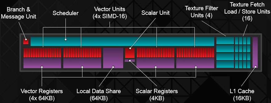
Again, the underlying GCN architecture on which Hawaii is based remains similar. The Compute Unit building block looks exactly the same, with 64 IEEE 754-2008-compliant shaders split between four vector units and 16 texture fetch load/store units.
There are a few tweaks to the design though, including device flat addressing to support standard calling conventions, precision improvements to the native LOG and EXP operations, and optimizations to the Masked Quad Sum of Absolute Difference (MQSAD) function, which speeds up algorithms for motion estimation. Incidentally, all of those features debuted alongside the Bonaire GPU we reviewed back in March (AMD Radeon HD 7790 Review: Graphics Core Next At $150); AMD just wasn’t discussing them yet. And with the introduction of DirectX 11.2, both Bonaire and Hawaii add programmable LOD clamping and the ability to tell a shader if a surface is resident—both of which are tier-two features associated with tiled resources.
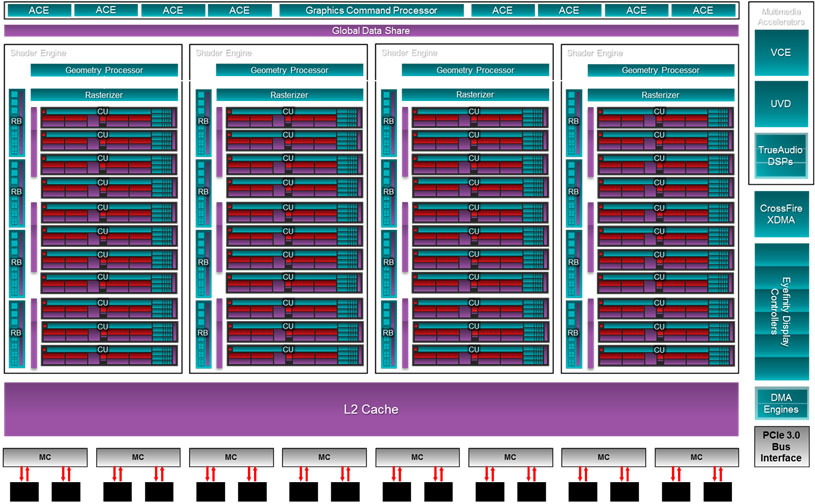
But the arrangement of AMD’s CUs is different. Whereas Tahiti boasted up to 32 Compute Units, totaling 2048 shaders and 128 texture units, Hawaii wields 44 CUs organized into four of what AMD is calling Shader Engines. The math adds up to 2816 aggregate shaders and 176 texture units. Operating at up to 1 GHz (this becomes an important distinction later), that’s 5.63 TFLOPS of floating-point performance. We've also come to learn that AMD changed the double-precision rate from 1/4 to 1/8 on the R9 290X, yielding a maximum .7 TFLOPS. The FirePro version of this configuration will support full-speed (1/2 rate) DP compute, giving professional users an incentive to spring for Hawaii's professional implementation.
Hawaii also employs eight revamped Asynchronous Compute Engines, responsible for scheduling real-time and background task to the CUs. Each ACE manages up to eight queues, totaling 64, and has access to L2 cache and shared memory. In contrast, Tahiti had two ACEs. The Kabini and Temash APUs we wrote about earlier this year come armed with four. Why is Hawaii so dramatically different? Some evidence exists to suggest that Hawaii’s asynchronous compute approach is heavily influenced by the PlayStation 4’s design, though AMD won't confirm this itself. Apparently, Sony’s engineers are looking forward to lots of compute-heavy effects in next-gen games, and dedicating more resources to arbitrating between compute and graphics allows for efficiencies that weren’t possible before.
Tahiti’s front-end fed vertex data to the shaders through a pair of geometry processors. Though its quad Shader Engine layout, Hawaii doubles that number, facilitating four primitives per clock cycle instead of two. There’s also more interstage storage between the front- and back-end to hide latencies and realize as much of that peak primitive throughput as possible.
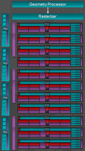
In addition to a dedicated geometry engine (and 11 CUs), Shader Engines also have their own rasterizer and four render back-ends capable of 16 pixels per clock. That’s 64 pixels per clock across the GPU—twice what Tahiti could do. Hawaii enables up to 256 depth and stencil operations per cycle, again doubling Tahiti’s 128. On a graphics card designed for high resolutions, a big pixel fill rate comes in handy, and in many cases, AMD claims, this shifts the chip’s performance bottleneck from fill to memory bandwidth.
The shared L2 read/write cache grows from 768 KB in Tahiti to 1 MB, divided into 16 64 KB partitions. This 33% increase yields a corresponding bandwidth increase between the L1 and L2 structures of 33% as well, topping out at 1 TB/s.
It makes sense, then, that increasing geometry throughput, adding 768 shaders, and doubling the back-end’s peak pixel fill would put additional demands on Hawaii’s memory subsystem. AMD addresses this with a redesigned controller. The new GPU features a 512-bit aggregate interface that the company says occupies about 20% less area than Tahiti’s 384-bit design and enables 50% more bandwidth per mm². How is this possible? It actually costs die space to support very fast data rates. So, hitting 6 Gb/s at higher voltage made Tahiti less efficient than Hawaii’s bus, which targets lower frequencies at lower voltage, and can consequently be smaller. Operating at 5 Gb/s in the case of R9 290X, the 512-bit bus pushes up to 320 GB/s using 4 GB of GDDR5. In comparison, Tahiti maxed out at 288 GB/s.
Current page: Hawaii: A 6.2 Billion Transistor GPU For Gaming
Next Page CrossFire: Farewell Bridge Connector; Hello DMA-
beta212 That's incredible. Especially at high res, I wonder how they do it. But the low price alone is enough to blow the competition away. Seriously think about it, it's around half the price for higher performance!Reply
- AMD: We're not aiming for the ultra high end.
I think Nvidia just got trolled. -
slomo4sho Great price point. This card has already broken world records just a few hours after release!Reply
-
esrever 2 of these for 4k looks amazing but Im a little disappointed by the power consumption when you crank up performance.Reply -
aznguy0028 I was thinking about hopping on the 7970ghz when it's on sale, but after seeing this, it's time to break apart the piggy bank for the 290x, what value!Reply -
Benthon Like the conclusion said, you just can't argue about aesthetics and thermals at this price point/performance. Well done AMD, lets see team green's response! Go consumer!Reply -
Shankovich Wow, and it's pegged at 73% too. Even if nVidia's "780ti" beats the 290X, it probably won't beat a 290X running at full power. And if mantle does make some big performance boosts, nVidia is going to be in a really tight spot. Looking forward to what they'll do. In the mean time, loving this competition! We all win in the end.Reply -
anxiousinfusion Wait the 290 X... X? is going to be $550?! Forgive me, padre for I have sinned.Reply


