AMD A10-7850K And A8-7600: Kaveri Gives Us A Taste Of HSA
We've spent the days following CES benchmarking two of AMD's new Kaveri-based APUs. Do the Steamroller x86 architecture, GCN graphics design, and HSA-oriented features impress, or do they come up short against Intel's value-oriented Haswell-based parts?
Enabling HSA On The Kaveri APU
Let’s get back to that concept of integration. Done right, integration should allow for compounding efficiencies. Subsystems brought closer together can communicate more quickly and save power.
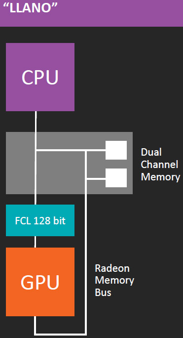
Back when AMD introduced its Llano APU, the company put four Stars cores, a northbridge, two 64-bit memory channels, PCIe control, and a graphics engine on one die. It provided a 128-bit Fusion Control Link to the GPU for access to coherent memory space, simultaneously giving the CPU access to the GPU’s frame buffer. Separately, another bus gave the graphics engine higher-bandwidth access to memory.
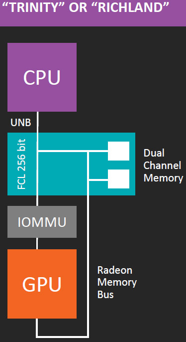
The advent of Trinity (and then Richland) saw AMD push integration even further. It unified the CPU and graphics northbridges, doubling the data path bandwidth of its Radeon Memory Bus in the process. Perhaps even more significantly, it added an I/O memory management unit, attached through the Fusion Control Link, which gave the GPU access to virtual address space. The road to HSA was slowly being paved.
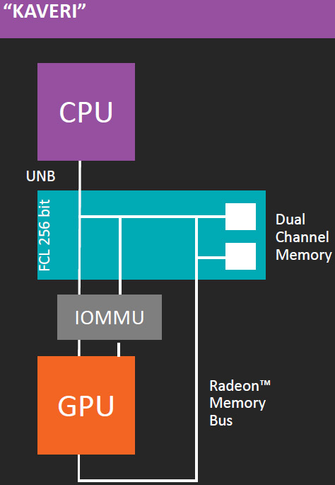
Kaveri incorporates a second bus through the IOMMU for coherency. It also exposes functionality called system-level atomics for synchronizing work across different cores. Together, those features complete the puzzle and enable a trio of HSA features.
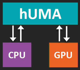
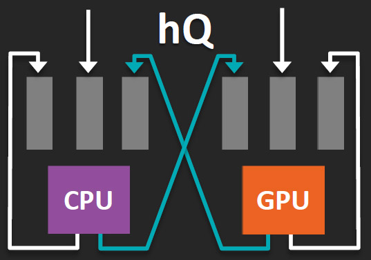
A heterogeneous unified memory architecture, to begin, gives the CPU and GPU subsystems visibility into the entire memory space, up to 32 GB. Additionally, both the CPU and GPU are treated equally by AMD’s heterogeneous queuing model. Work can be dispatched from one to the other and vice versa. As a result, the APU’s on-die resources can tag-team more compute-intensive workloads.
Right off the bat, AMD is identifying a handful of tasks that’ll benefit from greater compute potential in the mobile and desktop spaces. Media playback is the first. You’ve already seen us demonstrate how demanding H.265 encoding can be. AMD is going to offload encode/decode onto the GPU, since it wasn’t able to build a fixed-function accelerator for playback in time, and doesn’t expect to even try encoding that way. Unfortunately, the requisite software is still being worked on, so we can’t compare CPU- to GPU-based HEVC playback today. In the same vein, video and image editing already do lean on GPU resources (we have our own Photoshop, Premiere Pro, and After Effects tests that are technically OpenCL-optimized). This will naturally continue with Kaveri. Of course, gaming is that killer app always able to push the latest and greatest; developers are already using compute in a variety of ways. For example, DICE uses a compute shader for tile-based deferred rendering in Battlefield 4.
How Do I Use This HSA You Speak Of?
Get Tom's Hardware's best news and in-depth reviews, straight to your inbox.
AMD makes a big deal about its effort to design hardware that just works within the scope of how developers write code today, rather than forcing them to change direction yet again. Leveraging HSA shouldn't have the long adoption curve of multi-core CPUs, which were difficult to fully utilize, or GPGPU computing, which was only possible through low-level APIs for quite a while. Instead, the company’s HSA features map to OpenCL 2.0, ratified late last year.
The bad news is that the applications already installed on your PC aren’t optimized for Kaveri’s full feature set (though AMD does claim legacy OpenCL benefits from HSA thanks to run-time improvements). That’ll require ISVs to gradually introduce updated software. But a growing swath of developers is becoming increasingly proficient with OpenCL, and we’ve already incorporated a number of workloads into our benchmark suite able to leverage the API. Though testing won’t reflect HSA-oriented design today, we’re already working with a couple of big names to fold in relevant workloads.
Bottom line: we waited years for the first mainstream OpenCL-optimized applications, and now we have many well-known multimedia, content creation, productivity, and gaming titles benefiting from heterogeneous computing. We only expect to be on-hold for months before software starts showing up written for OpenCL 2.0. When that happens, AMD’s HSA features should augment performance and power consumption in different ways.
Current page: Enabling HSA On The Kaveri APU
Prev Page A More Capable GPU: GCN Surfaces In Kaveri Next Page Test Hardware And Software-
Someone Somewhere Yeah, almost all the diagrams refer to the 4760K.Reply
Given that AM3+ looks like it's done, it would have been nice to see a 6-core chip. Still, one of these may end up in my next laptop. -
spp85 A10-7850k is slower than A10-6800K ?? WTF. Its all hype than actual performance to the table. Even on OpenCL GPU accelerated apps doesn't have any advantage with A10-7850k over i5 or sometimes i3 CPUs. Hopeless is what I feel about AMD CPUs.Reply -
Someone Somewhere Reply12454254 said:A10-7850k is slower than A10-6800K ?? WTF.
I got the opposite impression. Which graph are you looking at? -
Jaroslav Jandek Thank you for the article (especially the power consumption measurements), Chris. It is definitely an improvement over Richland but kind of boring (disappointingly expectable).Reply
I really like where AMD is going (HSA, GCN and TrueAudio).Too bad the manufacturing process of GlobalFoundries just can't match Intel's.
Also, it would be interesting to see the new Bay Trail Pentium or Celeron CPUs (whichever is closer in performance) in the Efficiency graphs. -
Someone Somewhere I'm fairly sure that this is on TSMC's 28nm node. GlobalFoundries can't do that yet; this is on the same process used for AMD GPUs currently.Reply -
Jaroslav Jandek Reply
28nm SHP from GlobalFoundries. AMD bought over $1 billion worth of wafers from them in december...12454280 said:I'm fairly sure that this is on TSMC's 28nm node. GlobalFoundries can't do that yet; this is on the same process used for AMD GPUs currently.
I guess you have been reading the articles from a year ago about AMD still using TSMC despite promises of GlobalFoundries' new 28nm SHP process. -
jacobian I don't really believe into the whole HSA smoke-screen. By the time HSA-enabled apps take off, you will be ready to upgrade from your CPU again. The one terrible truth that stands out right now is that at current prices, the flagship Kaveri A10 doesn't make any sense whatsoever. Kaveri A8? Maybe. Richland A10-6790K? Perhaps. But the Kaveri A10 at $180 is a just a joke, specially after all that hype.Reply -
Someone Somewhere CPUs are usually released at ridiculous prices, and come down over a month or two.Reply
