The AMD A8-3500M APU Review: Llano Is Unleashed
Code-named Llano, AMD’s first desktop-class APU arrives today. This single-chip combination of the Stars CPU architecture and Radeon graphics brings unique strengths (and weaknesses) to the table, and we’re here to compare them to Intel's Sandy Bridge.
The West-Side CPU
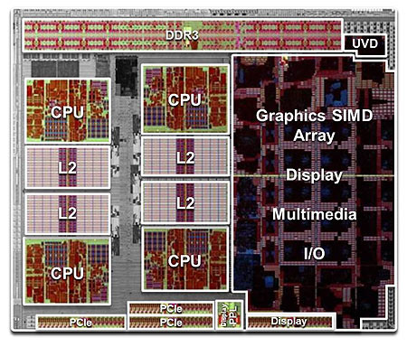
The CPU portion of Llano’s die is based on the Stars architecture we know from the original Phenom, living on in today’s Athlon II and Phenom II processors. There are a few notable differences and improvements, though. The most obvious is AMD’s transition from 45 nm manufacturing to a 32 nm node. So, right out of the gate, we expect certain power- and thermal-oriented advantages compared to the same piece of logic manufactured at 45 nm. We don’t have that here, of course. Adding the Fusion-oriented components just about doubles Llano’s transistor count compared to Deneb, adding up to 1.45 billion.
Bear in mind that Sandy Bridge-based CPUs already employ a mature 32 nm process, and Intel is on the verge of making a shift to 22 nm with the Ivy Bridge die shrink later this year. AMD knows that Intel has a manufacturing technology advantage and is looking to compensate in other ways.
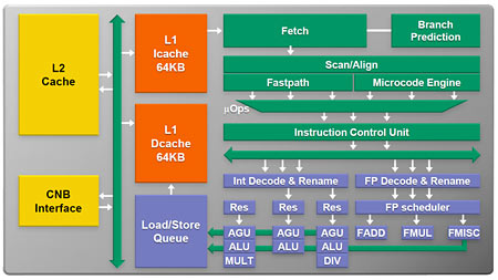
AMD claims that Llano’s processing cores demonstrate an average 6% improvement in successfully executed instructions per clock (IPC) versus previous Stars-based offerings. In some cases there will be zero improvement and in others the new core might show as much as a 15% increase. There are two main reasons for this on-average performance improvement: more L2 cache and a better hardware prefetcher.
Article continues belowAs you likely noticed, the 6 MB shared L3 CPU cache is gone entirely, a loss AMD hopes will be mitigated by a doubling of the exclusive L2 cache from 2 MB to 4 MB, totaling 1 MB of dedicated cache per core. This might sound like a dire compromise at first, but keep in mind that although a large L3 on the back of the northbridge allows sharing of another high-speed repository between cores, it also increases latency and presents a problem for power management. Increasing the L2 might sacrifice a little overall scalability, but it helps augment multithreading operations and allows more granular control of the chip’s power management. Since this was one of the main goals of Llano’s design team, the change made sense. And although the L2 and L3 cache configurations are changed, each core has the same 64 KB L1 instruction and data cache (128 KB total L1) as the 45 nm Phenom II and Athlon II families.
AMD also put a lot of work into its hardware prefetcher. Traditionally, a hardware stride prefetcher looks at specific memory instructions over time, and if the address loaded differs by a constant stride, the prefetcher may decide that it’s beneficial to put that instruction into the cache. The problem with this approach is that many programs can make it difficult to extrapolate patterns because of spurious instructions that distract the algorithm. AMD enhanced the prefetcher intelligence with Instruction Pointer (IP)-based prefetching. IP understands the instructions accessing the memory and uses that intelligence to find patterns, improving its ability to find strides.
Aside from this, the buffer sizes are larger. The reorder buffer is about 20% larger and the load/store buffers are doubled in size. We’re also told that the hardware multiplier is better, but AMD won’t disclose exactly what it improved.
When all is said and done, the 6% average IPC increase over the Phenom II represents a modest gain, if it’s quantifiable at all in testing. It seems that improving CPU performance was not a major target for the design team. And again, this makes well-enough sense to us with the first Bulldozer-based CPU (Zambezi) in the wings.
Get Tom's Hardware's best news and in-depth reviews, straight to your inbox.
Power management takes precedence, which is smart since Llano needs to share its thermal ceiling between the CPU and GPU. While the aging Stars architecture might be sufficient to show what the GPU side can do today, this APU’s successor replaces Stars with Bulldozer-derived silicon. That part may be the what manages to challenge Intel on the processor side. AMD’s Rick Bergman showed off a Trinity-based APU at this year’s Computex and said the first silicon was showing up at the lab. Hopefully the company isn’t late with that part.
Don Woligroski was a former senior hardware editor for Tom's Hardware. He has covered a wide range of PC hardware topics, including CPUs, GPUs, system building, and emerging technologies.
-
fstrthnu AMD is kind of in a fix here, the more enthusiast gamers won't even bother looking at the Llano computers while this is kind of overkill for casual gamers. MAYBE money-pressed college students or something, but most people will just skip this and either buy a regular gaming computer or build their own using one of the guides from this very site! Going for good graphics in cheap desktops is kind of a futile exercise, the people who will care will just get the more expensive stuff anyways. Notebooks are more understandable, but the prices on the decent gaming desktops are just too good for Llano to be very competitive (and also, the CPU portion will be a letdown for the average person. Noticeably slower than the comparable Intel Core i5.)Reply -
stingstang Good job, AMD. You finally made a better cpu/gpu combo than intel in terms of graphics power.Reply
....big win there... -
vz7 After reading the desktop benchmarks on anandtech I can't say I'm impressed. The top of the line a8 3850 manages to scratch the best intel integrated graphics, which doesn't say much. Its CPU power seems to be a toss up with the i3. I think this hardly justifies the +70 premium (over an i3) that you'd have to spend to get it.Reply -
billj214 This APU being somewhat low power and good graphics almost deserves to be in a tablet PC since CPU processing is not critical in tablet PC's and graphics is something that can help with media and games.Reply
Ditto on the "Good Job AMD" definitely on the right track. -
cangelini vz7Do you know when the desktop review for llano will be out?Reply
The NDA is up on the 30th. -
niceview two things:Reply
1) What happened to the Game Charts results for the Radeon HD 5570, when the games were benchmarked? I thought you made a point to say you were going to compare the APU's 6620G with a discrete card (that has the same number of SPs and same clock). So much for that, unless you thought only comparing the two with a synthetic test was enough. Oh well. Tom's can be such a tease!
2) I'm just a little disappointed that the APU's graphics power was not able to double Intel's.... Under the best of circumstances, AMD's latest integrated graphics came close to being twice as fast, but i guess that is ok since we are not playing horseshoes. I just thought it would be nice if it had made a nice even doubling, or more. Now, i'm worried IVY BRIDGE will beat it.... -
niceview sorry, i guess that should be:Reply
we ARE playing horseshoes...
and i have to give credit where credit is due: props to AMD for almost doubling Intel's HD Graphics in the integrated space....

