The AMD A8-3500M APU Review: Llano Is Unleashed
Code-named Llano, AMD’s first desktop-class APU arrives today. This single-chip combination of the Stars CPU architecture and Radeon graphics brings unique strengths (and weaknesses) to the table, and we’re here to compare them to Intel's Sandy Bridge.
CPU + GPU = APU: East Meets West
We can see that the CPU and GPU hardware aren’t much different from what AMD already has in the market. But what makes the Fusion initiative unique is the combination of these two strengths in a single package. Company representatives stress that the challenge of Llano was to get everything working together in the best and most power efficient way. That comes down to the plumbing.
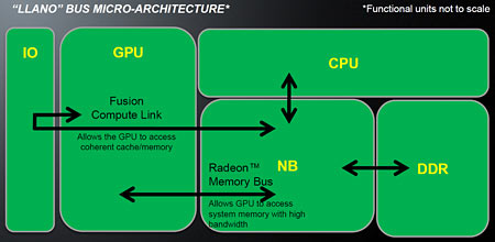
There are five main components of Llano that have to communicate with each other: the CPU complex, the GPU complex, the northbridge, the traditional I/O block, and the DDR memory I/O block. The CPU-to-northbridge link isn’t anything new, so let’s talk about what we haven’t seen yet: namely, the GPU-to-northbridge links. Because there are two GPU usage scenarios, it has two dedicated links.
The first link is called the Radeon memory bus. It’s no secret that poor bandwidth equals poor graphics performance, so the GPU can’t rely on the same memory interface as a typical CPU. The Radeon memory bus is a direct path from the GPU through the northbridge to the DDR memory, and it provides priority access to RAM for high-bandwidth operations. AMD’s chief engineer Mike Goddard made it clear that this link is absolutely essential to extract discrete-class graphics performance from the Llano APU.
Article continues belowBut there is a second link that the GPU needs, and this is one of the components that really makes Llano an APU instead of just a CPU and a GPU on the same die: the Fusion compute link. Traditionally, I/O devices have been able to go through the PCI Express interface to access the CPU’s cache. This is a bottleneck for GPU compute operations, so AMD augmented this path and gave the GPU better access to share data with the CPU or to extract memory contents from that shared pool. The Fusion compute link is the piece that allows Llano to extract compute performance at a very efficient power level.
Power Management
One of the three main features of Llano is what the chip company brands AMD AllDay Power. AMD considers the mobile market an ideal place for the APU, so it makes sense that power efficiency is high on its priority list. So, how is this achieved on the A-series?
There are two main voltage rails responsible for Llano’s power usage: the VDD rail (shared across the CPU cores) and the VDDNB plane (shared across the GPU, UVD block, graphics memory controller, and northbridge).
Get Tom's Hardware's best news and in-depth reviews, straight to your inbox.
At first you might assume that sharing the single VDD voltage rail across four CPU cores might not be the most efficient way to control power when the operating system may often only require cycles from one. But this single supply has two modes: Core C6 (CC6 mode) and Package C6 (PC6 mode). CC6 mode is capable of powering down individual CPU cores, while PC6 mode is able to lower the power on the entire rail. This provides the granularity needed to best handle a variety of situations.
The VDDNB plane is a bit more complex, as it’s responsible for a number of components. From a pure efficiency standpoint this isn’t an ideal situation because the whole rail has to run at the highest common voltage—that is to say, the highest voltage required by any one of these components at a time. This design decision was chosen because breaking it out of the package and adding regulators would increase cost. As a result, the voltage and frequency P-states vary based on a number of factors: the northbridge P-state, the GPU P-state (something usually controlled by the driver, but that also can be altered through hardware), the PCI Express speed (if a second-gen PCIe device is present it drives a higher voltage requirement), and the UVD workload.
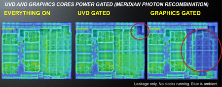
But while voltage is shared, there remains significant granularity in which components can be gated. The GPU portion can be powered down if idle time goes past a programmable threshold, or if the driver detects and responds to usage. The graphics memory controller is capable of using significant amount of power, so it can be turned on and off as required. The UVD block can also be used or gated as needed.
There are some display power optimizations in play here, too. Standard frame buffer compression is used, of course. But AMD enhanced the adaptive backlight modulation (ABM) component. This can analyze the image that is to be shown and tweak the backlight and brightness levels to display an image as close to the original as possible using the least amount of power.
The following images show how specific portions of the APU can be bypassed: blue is ambient and green is active. These are only a few examples, as other components like the CPU cores can also be controlled.
Turbo Core
Turbo Core is nothing new. AMD included this frequency-boosting feature as far back as its Phenom II X6 introduction. What’s different is that Llano balances GPU and CPU resources to fit within the chip’s TDP.
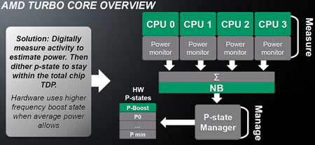
AMD’s Mike Goddard stressed that the company’s approach to this feature is unique in that it is primarily based on digital performance measurements, not analog thermal readings. The APU’s digital APM (Advanced Power Management) module measures activity to estimate power requirements and dithers the P-state to stay within the chip’s TDP. The benefit of this approach should be consistent and repeatable performance compared to one primarily based on temperature measurements. Of course, the downside would be that performance headroom might not be fully utilized if the APM underestimates headroom versus actual temperature limitations.
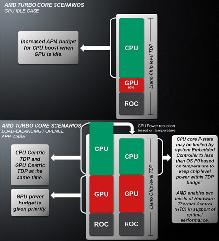
In any case, when the APM decides that headroom is available, it invokes an OS-invisible state called “P boost” that increases clocks on the CPU-side. Keep in mind that Llano’s GPU cannot be accelerated beyond its shipping speed (it can, however, be throttled down to cut power and minimize heat)—only the CPU clock can be boosted. It’s also important to note that the GPU always takes precedence, so whenever there’s a graphics load, the CPU has less opportunity to see the benefit of Turbo Core.
But there’s a final piece to the puzzle. While temperature is not the primary determining factor of P-state, it remains an important failsafe. There is one scenario where both the CPU and GPU can be stressed beyond Llano’s TDP: when it comes to load-balancing an OpenCL compute application. Because the GPU is more effective at this type of task, it is once again given priority. But the CPU also pushes against its limit, and if the temperature exceeds that barrier, the CPU can drop to less than P0—for instance, P1 or P2—in order to bring temperatures down. We were told that this is the only scenario where Llano operates its processing cores below their nominal speed, but it can happen.
Unfortunately we’re unable to test any of those scenarios because no tools exist that report the true clock speed of Llano’s CPU cores. Even the monitoring utility AMD gave us incorrectly reports the CPU clock as its nominal level, without ever seeing the effect of Turbo Core when the GPU is idle. Clearly, it’s important to validate the company’s claims, as we’d like to see first-hand what scenarios can force the APU to throttle back. You can be certain that we will revisit this issue as soon as we figure out a way to properly measure what is going on inside the Llano APU under different loads.
As mentioned, though the CPU clocks can scale up and down, the graphics engine won’t exceed its factory speed; it cannot be pushed any further by Turbo Core. According to AMD, this may change in the future. Our interpretation is that the upcoming Trinity architecture may feature the flexibility to accelerate graphics performance when the CPU cores have thermal headroom to give up.
Current page: CPU + GPU = APU: East Meets West
Prev Page The East-Side GPU Next Page The Driver Interface And AMD Steady VideoDon Woligroski was a former senior hardware editor for Tom's Hardware. He has covered a wide range of PC hardware topics, including CPUs, GPUs, system building, and emerging technologies.
-
fstrthnu AMD is kind of in a fix here, the more enthusiast gamers won't even bother looking at the Llano computers while this is kind of overkill for casual gamers. MAYBE money-pressed college students or something, but most people will just skip this and either buy a regular gaming computer or build their own using one of the guides from this very site! Going for good graphics in cheap desktops is kind of a futile exercise, the people who will care will just get the more expensive stuff anyways. Notebooks are more understandable, but the prices on the decent gaming desktops are just too good for Llano to be very competitive (and also, the CPU portion will be a letdown for the average person. Noticeably slower than the comparable Intel Core i5.)Reply -
stingstang Good job, AMD. You finally made a better cpu/gpu combo than intel in terms of graphics power.Reply
....big win there... -
vz7 After reading the desktop benchmarks on anandtech I can't say I'm impressed. The top of the line a8 3850 manages to scratch the best intel integrated graphics, which doesn't say much. Its CPU power seems to be a toss up with the i3. I think this hardly justifies the +70 premium (over an i3) that you'd have to spend to get it.Reply -
billj214 This APU being somewhat low power and good graphics almost deserves to be in a tablet PC since CPU processing is not critical in tablet PC's and graphics is something that can help with media and games.Reply
Ditto on the "Good Job AMD" definitely on the right track. -
cangelini vz7Do you know when the desktop review for llano will be out?Reply
The NDA is up on the 30th. -
niceview two things:Reply
1) What happened to the Game Charts results for the Radeon HD 5570, when the games were benchmarked? I thought you made a point to say you were going to compare the APU's 6620G with a discrete card (that has the same number of SPs and same clock). So much for that, unless you thought only comparing the two with a synthetic test was enough. Oh well. Tom's can be such a tease!
2) I'm just a little disappointed that the APU's graphics power was not able to double Intel's.... Under the best of circumstances, AMD's latest integrated graphics came close to being twice as fast, but i guess that is ok since we are not playing horseshoes. I just thought it would be nice if it had made a nice even doubling, or more. Now, i'm worried IVY BRIDGE will beat it.... -
niceview sorry, i guess that should be:Reply
we ARE playing horseshoes...
and i have to give credit where credit is due: props to AMD for almost doubling Intel's HD Graphics in the integrated space....


