AgileX In-Depth: PCIe Gen 5, DDR5, HBM3 and Optane DIMM Support
The Logic Continuum and Closing Thoughts
Innovation Race at the Edge, Comms, and Cloud
Ever since Intel's Bob Swan (now CEO) took over as CFO in late 2016, Intel has consistently shifted its messaging towards becoming a data-centric company. FPGAs fall coherently into that picture by being workhorses for processing, storing and moving data. In fact, with 5G, AI and IoT and all the ways data is being created, Intel believes that it is in the largest FPGA adoption cycle in history.
This massive amount of data is causing what Intel calls an innovation race. From the edge to the network to the cloud, companies are racing to innovate and get solutions to market as fast as possible. FPGAs are ideal for these workloads and afford a faster time to market, while still allowing companies to provide customized solutions.
Custom Logic Continuum
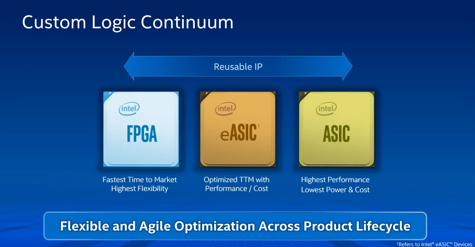
Intel’s goal, however, is to support customers throughout the whole lifecycle of a solution. As the pace of innovation slows down, customers will start focusing more on power, performance, and cost. This is where Intel positions eASIC, a company it acquired last year that designs structured ASICs. Those chips combine some characteristics of FPGAs and ASICs. For instance, eASIC's design time is closer to an FPGA, and the chips capture some of the power and performance benefits of an ASIC. But on the downside, they lose programmability.
The eASIC eventually paves the way for a fully-custom ASIC design. Intel also has design teams working to fulfill its goal to be part of the whole lifecycle of a product from programmable to custom. This is what Intel calls the "custom logic continuum" that it claims no other vendor can provide.
The key is the reusable IP. You begin with the FPGA, move to an eASIC, and lastly port it to an ASIC. Intel plans to evolve all three of these families. eASIC is currently fabbed on the 28nm process, but they can be built on various nodes. Intel tells us to expect to hear more about its plans for eASICs in the second half of the year.
While Intel does not forget its core embedded markets of old, it sees the edge, networking, and cloud as the three main catalysts for further FPGA adoption. Each of those categories leverages both the core value proposition of an FPGA, like time to market, programmability, and some additional aspects.
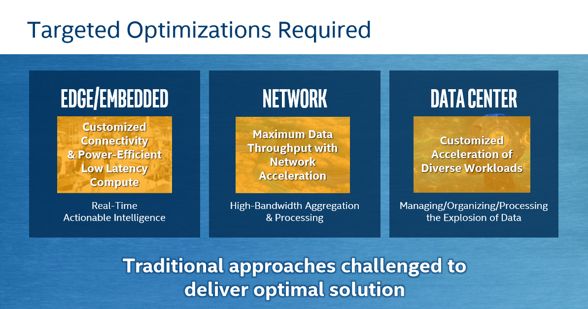
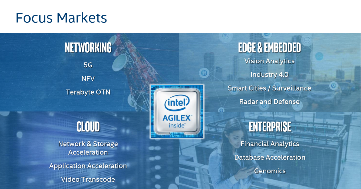
At the edge, it’s all about delivering real-time, low latency intelligence and data processing, such as frame-by-frame video processing. In the communications infrastructure market, FPGAs accelerate diverse packet-processing applications that require copious amounts of bandwidth. Obviously, cloud use-cases are even more diverse. But for the cloud service providers themselves, they want to rent clock cycles to their customers, so every clock cycle used for something else is wasted. For them, FPGAs can be used for infrastructure offload applications.
Get Tom's Hardware's best news and in-depth reviews, straight to your inbox.
To sum up, Intel’s goal is to drive ultimate capabilities in agility, flexibility, and scalability to move, store and process data, for which FPGAs are the first step in the custom logic continuum.
Closing Thoughts
Intel has brought a long laundry list of new features and capabilities to AgileX. As the first FPGA conceived from the ground up as part of Intel, Intel’s Programmable Solution Group has done a surprisingly good job at aligning their development with Intel's broader, data-centric strategy. This is evident from support for Optane Persistent Memory, Bfloat16, memory-coherency with Xeons via the CXL interconnect, and support for OneAPI.
Altera was already an Intel foundry customer and used its EMIB interconnects for the previous-gen Stratix 10, but it looks like Intel can really take heterogeneous integration to the next level with AgileX. It’s early days, but Intel envisions a whole ecosystem of both standard and custom chiplets from eASIC that it can connect via EMIB to personalize the FPGA.
Intel's acquisition of eASIC together with its existing ASIC teams also gives it the opportunity to be part of the complete custom logic continuum lifecycle, which is a unique capability. It will probably take time for Intel to build this ecosystem out, but we can already see one big benefit with the new memory coherency with Xeon. This functionality is built upon the PCIe 5.0 CXL interconnect, but Intel expects CXL to come to market in 2021, well after the initial AgileX launch. The mix-and-match design allows Intel to add the memory coherency capability later without respinning the entire FPGA. It should be clear this goes far beyond simply adjusting the number of chiplets connected to an I/O die as some of Intel's competitors do.
The base FPGA should provide a hefty performance and power improvement through the benefits of the 10nm process, second-gen Hyperflex architecture, and increased DSP capabilities for both floating-point and integer operations (which go as low as INT2). Intel also ticked the boxes for DDR5, HBM3, and 112G transceivers. The base die also contains a quad-core A53 CPU.
Intel hopes this combination of capabilities will provide the most flexible, scalable, and agile FPGA for the data-centric world as AI, 5G and IoT fuel an explosion of data that Intel says will spur the largest adoption cycle of FPGAs in its history. From what we’ve seen, the amount of technology packed into AgileX is impressive. The design touches virtually every asset of Intel’s portfolio, with OneAPI serving as the cornerstone that ties Intel’s portfolio together for all software developers.
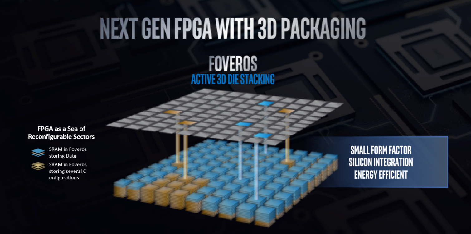
Lastly, at the Architecture Day in December, Intel showed a concept of an FPGA as a “sea of reconfigurable sectors.” This design stacks several layers of FPGA via Intel’s new 3D packaging technology Foveros on a 7nm process. As one last tidbit that we got from our briefing, Intel described Foveros as “Phase 2” of AgileX. As Dan McNamara, SVP of the Programmable Solutions Group, confirmed: “We’re looking at that for future derivatives of AgileX.” To what extent Intel will use Foveros in Phase 2 is unclear, but it’s clear there is more to come.
MORE: Best CPUs
MORE: Intel & AMD Processor Hierarchy
MORE: All CPUs Content
Current page: The Logic Continuum and Closing Thoughts
Prev Page OneAPI and the AgileX Family