Why you can trust Tom's Hardware
Second-Gen 3D V-Cache Technology AMD Ryzen 9 7950X3D
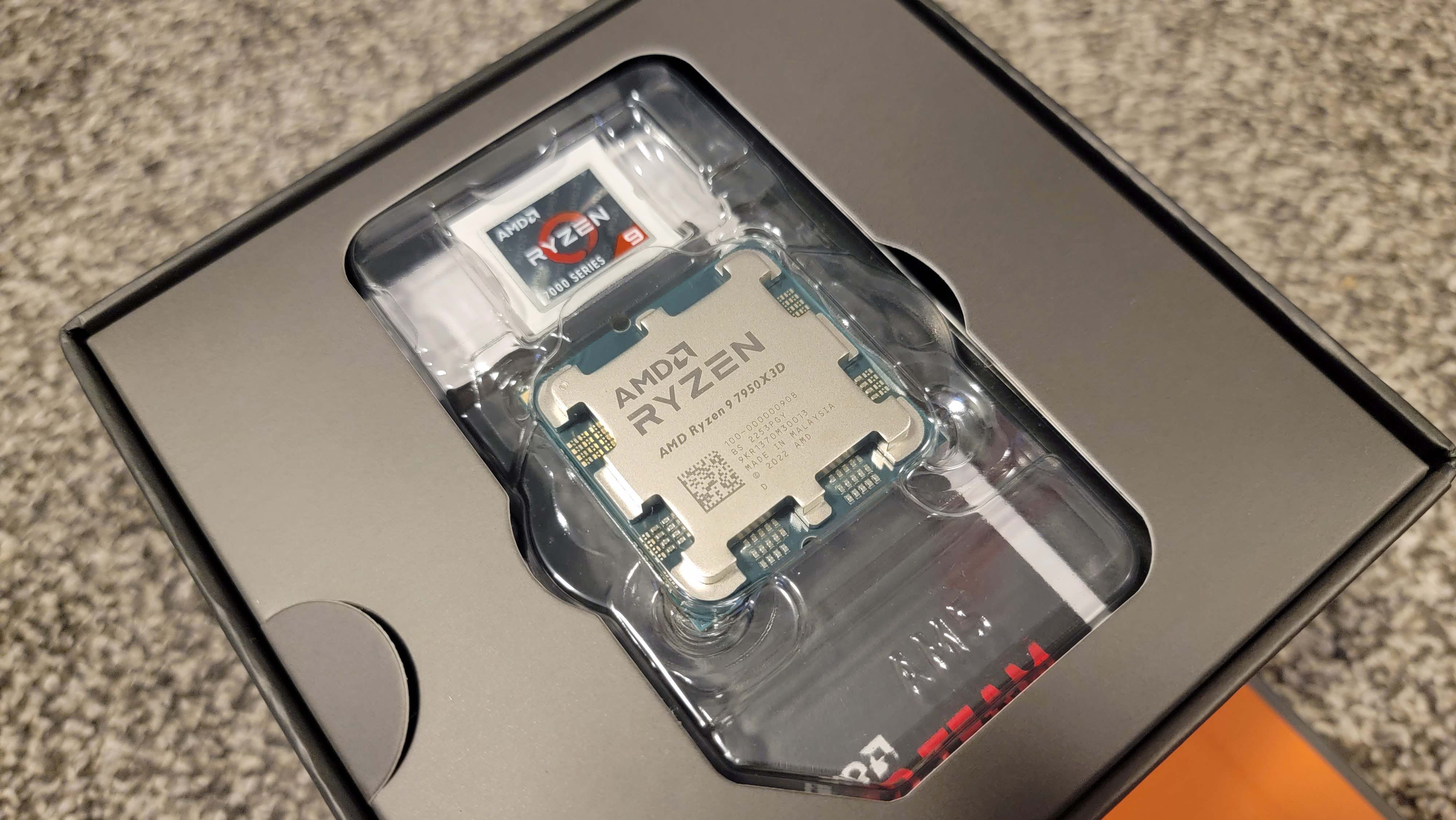
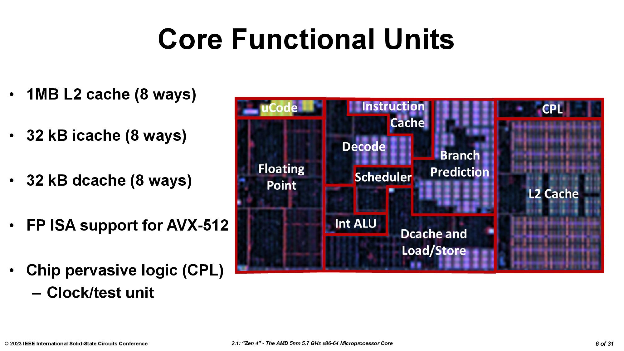
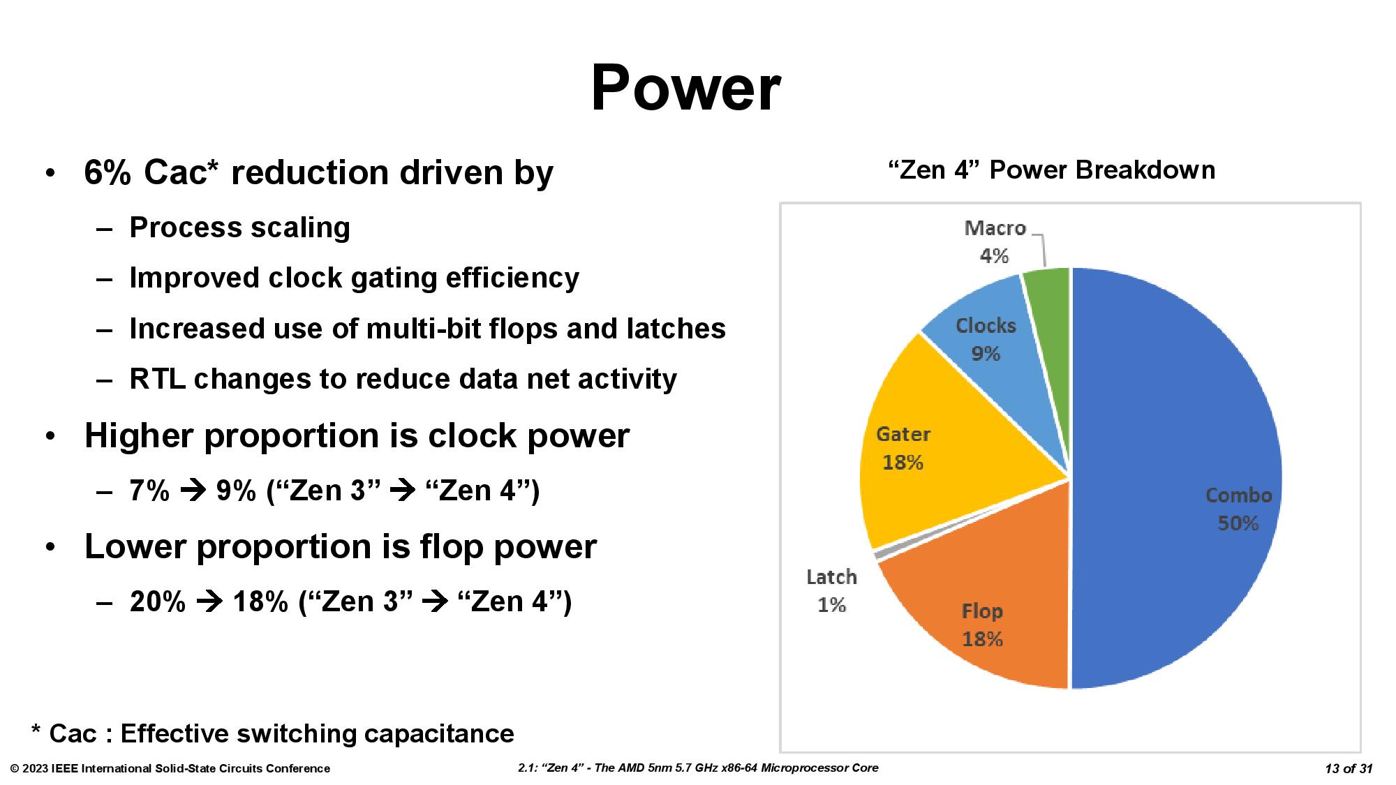
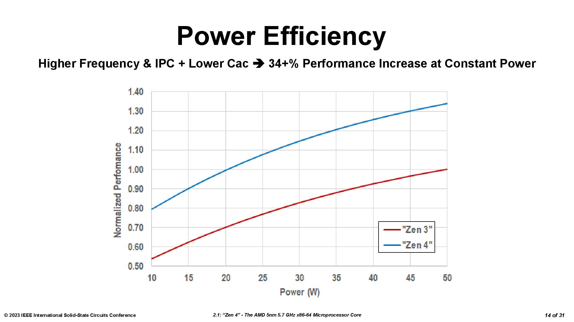
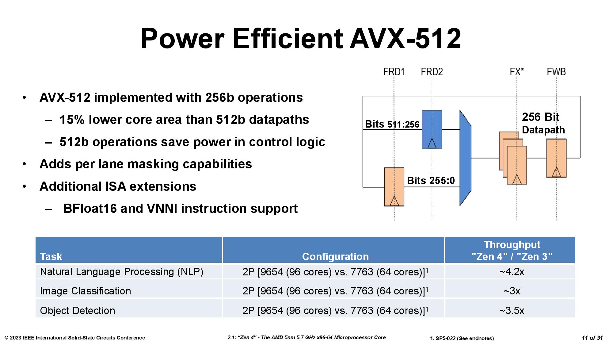
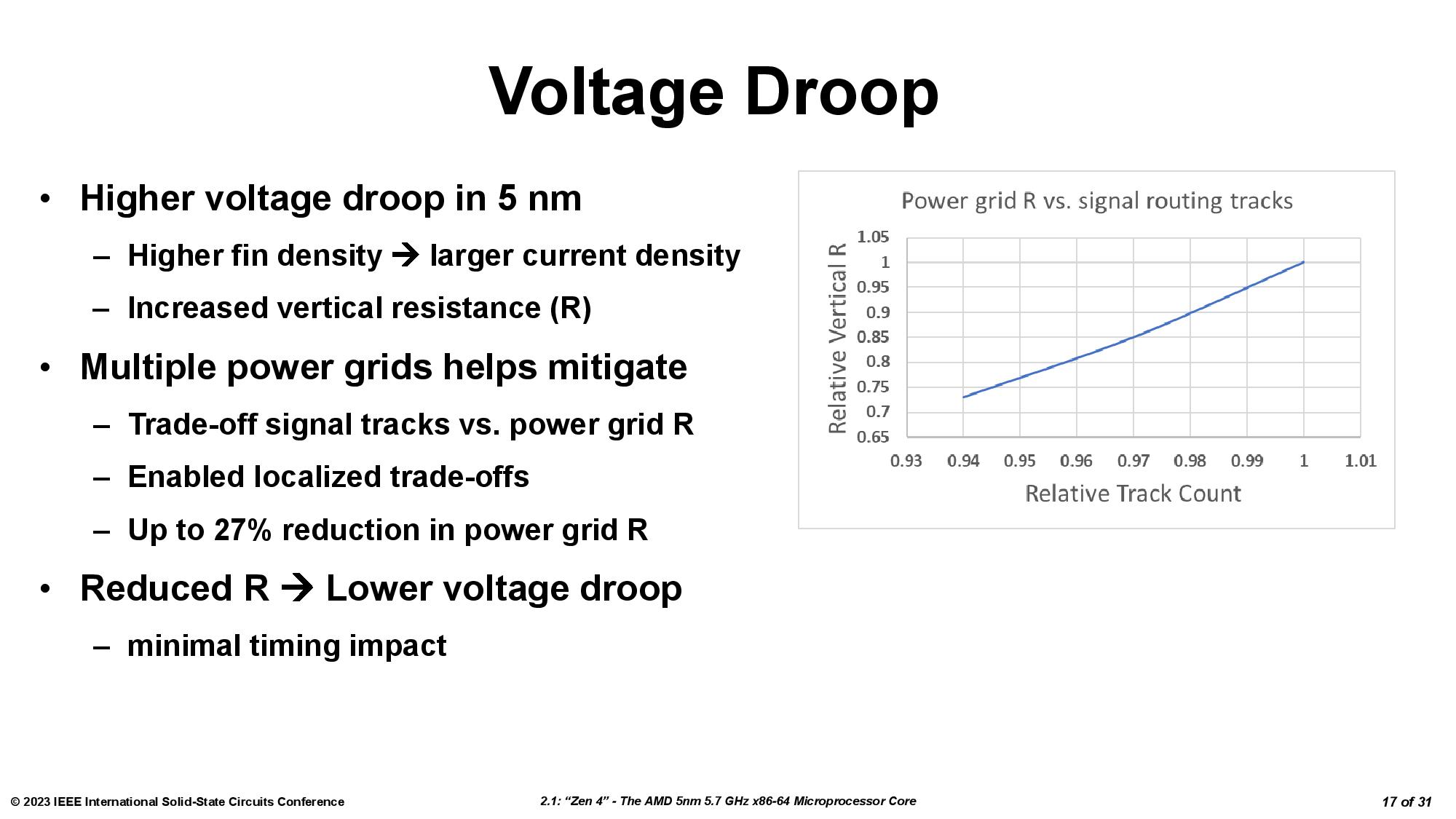
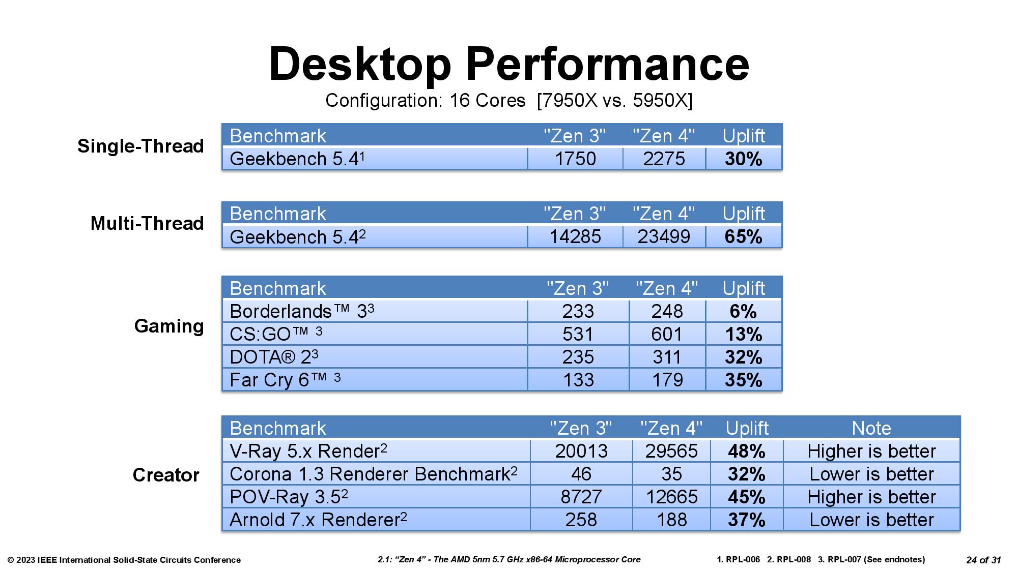
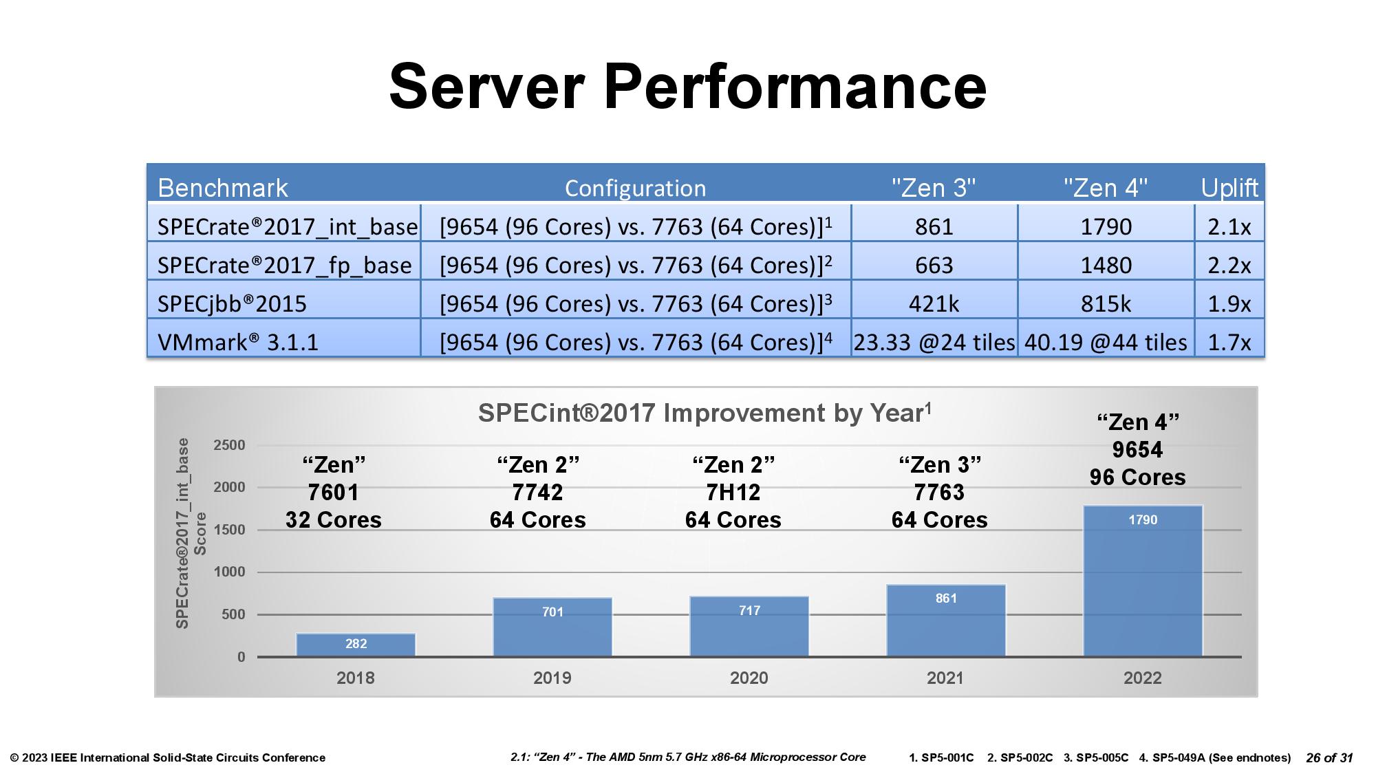
AMD didn’t share any details about its second-gen 3D V-Cache in its Ryzen 9 7950X3D briefing materials, but we found some details at the 2023 International Solid-State Circuits Conference (ISSCC) in AMD’s latest presentation on the Zen 4 architecture, and AMD has also answered a few of our follow-up questions and shared important new details, including that the chiplet remains on the 7nm process and now has a peak bandwidth of up to 2.5 TB/s, whereas the first-gen 3D V-Cache peaked at 2 TB/s (among lots of other new info). We also have new pics and diagrams of the new 6nm I/O Die that AMD uses for its Ryzen 7000 processors.
AMD has moved to the second-gen of its 3D V-Cache, and Intel doesn't have a competing tech. Overall, AMD's second-gen 3D V-Cache technology is an impressive step forward over the first-gen because it allows the company to leverage the now-mature and less-expensive 7nm process node to boost the performance of its cutting-edge 5nm compute die. The new design represents AMD taking the key advantage of chiplet-based design methodologies — using an older and less-expensive process node in tandem with expensive new process tech — into the third dimension.
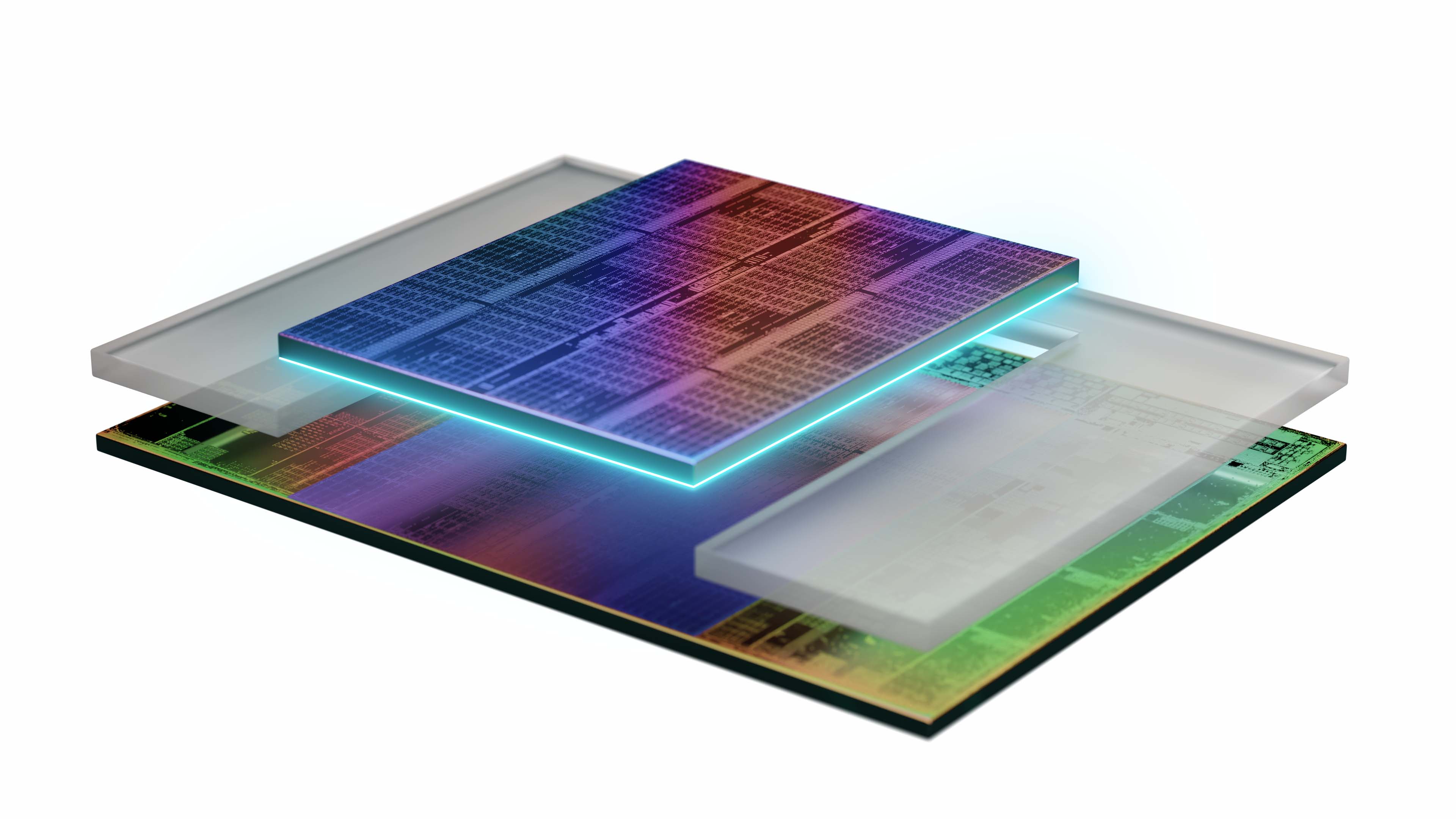
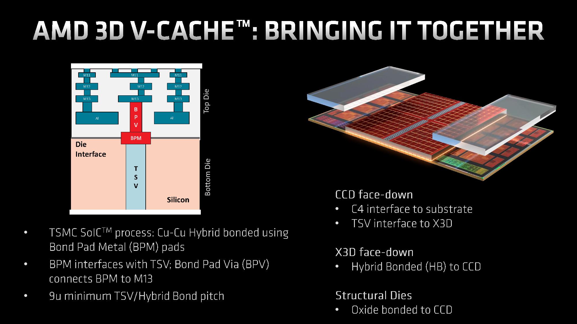
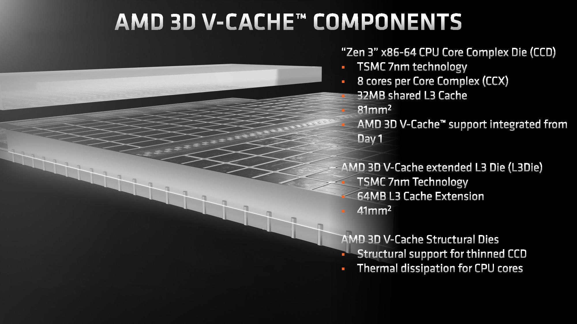
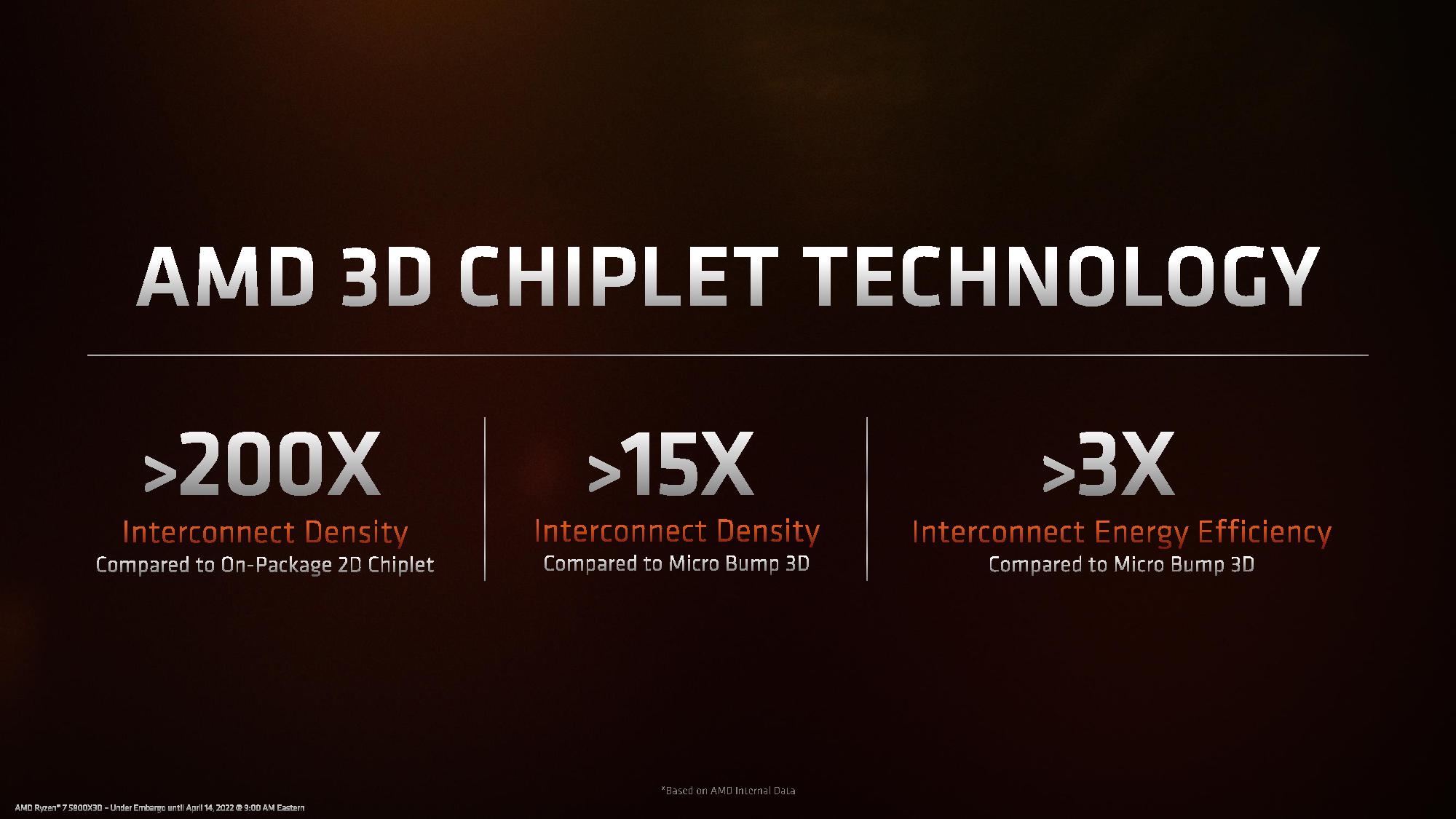
*The above album contains images of the first-gen 3D V-Cache implementation for illustrative purposes.
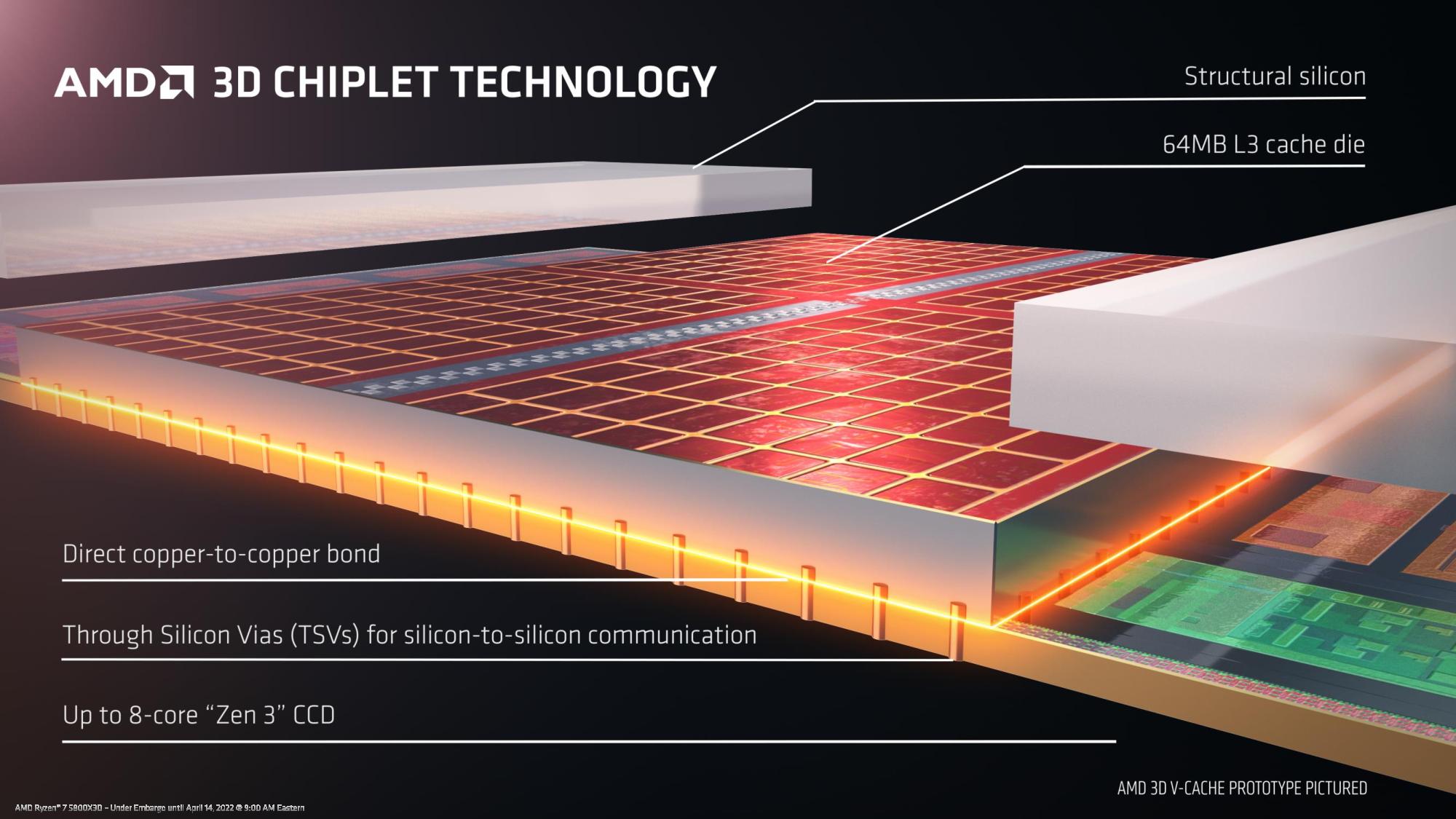
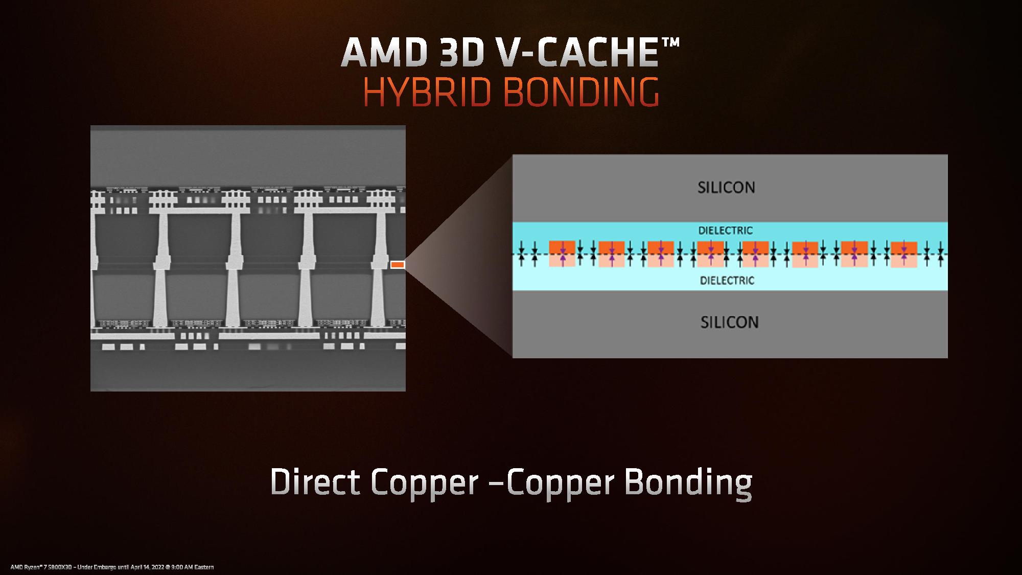
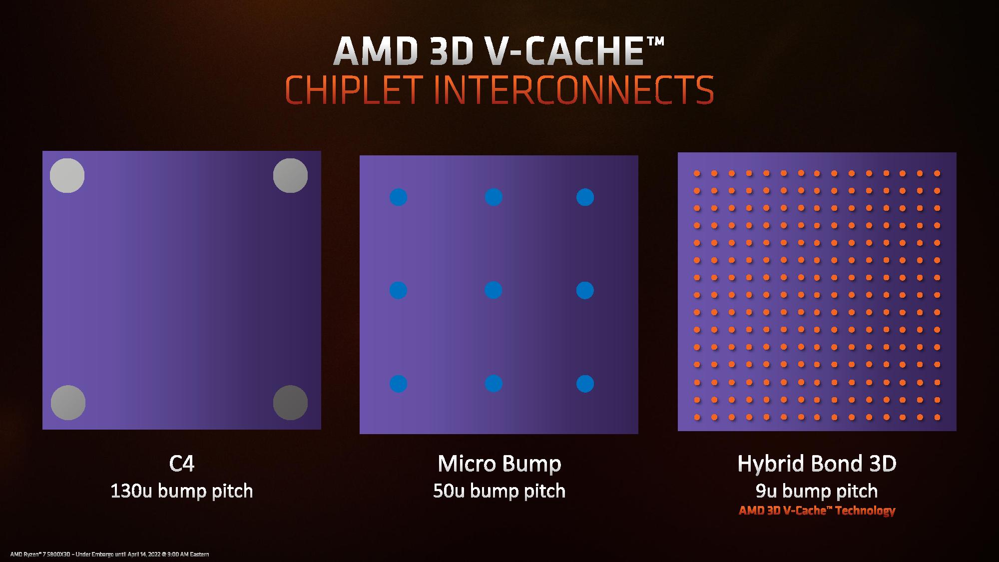
First, a quick high-level refresher. AMD’s 3D V-Cache tech stacks an additional SRAM chiplet directly in the center of the compute die (CCD) to isolate it from the heat-generating cores on the sides of the chiplet. AMD's 3D chip stacking tech is based on TSMC's SoIC technology. TSMC's SoIC is a bump-less chip stacking tech, meaning it doesn't use microbumps or solder to connect the two dies. Instead, the two dies are milled to such a perfectly flat surface that the TSV channels can mate without any type of bonding material. We’ve covered the deep-dive details of the first-gen 3D V-Cache technology in our 5800X3D review, and you can read much more about the hybrid bonding and manufacturing process here.
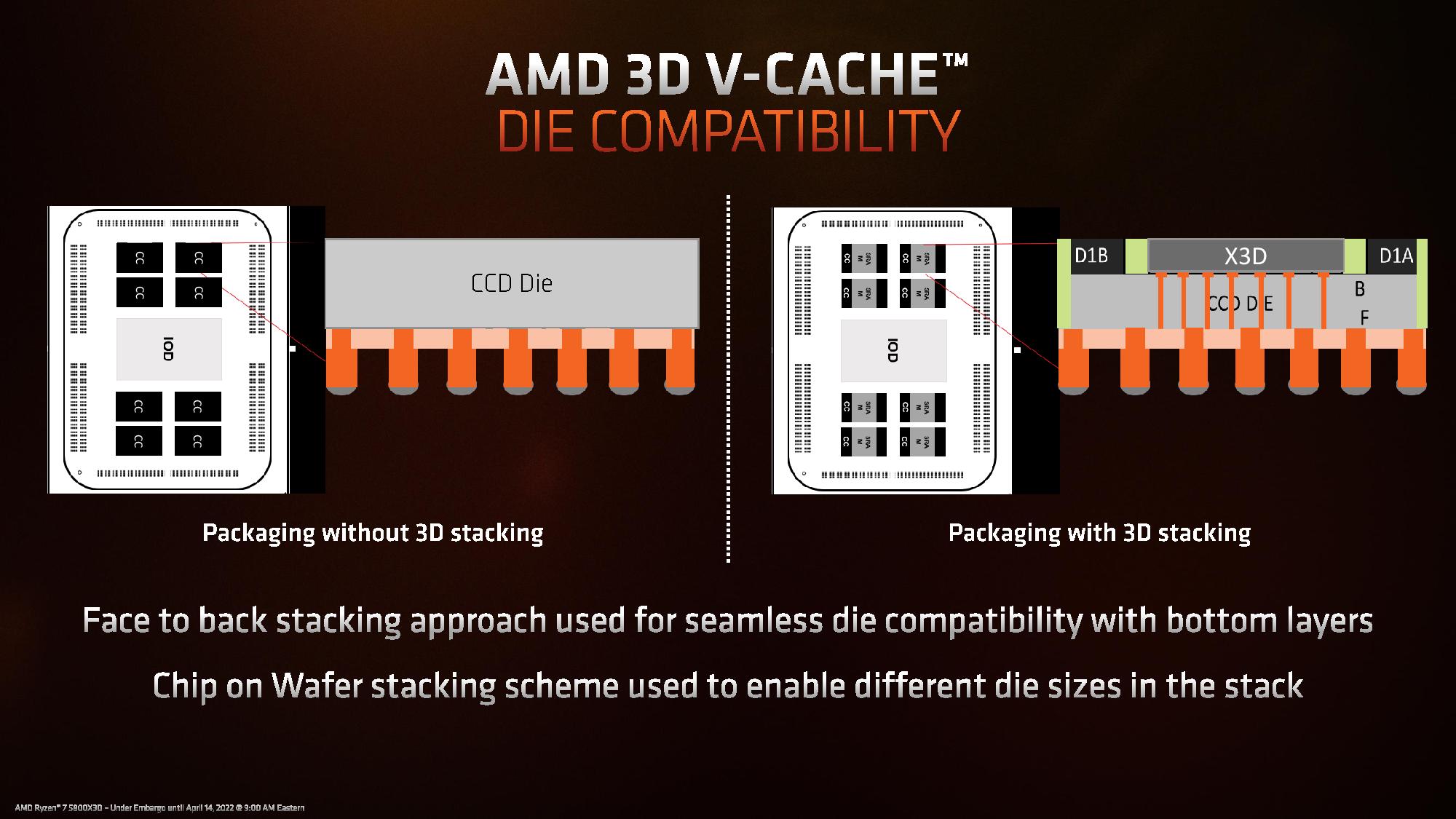
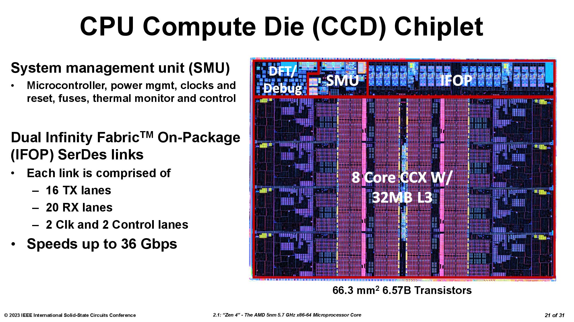
Now for the new stuff: AMD’s previous-gen 3D V-Cache used a 7nm L3 SRAM chiplet stacked atop a 7nm Zen 3 CCD. AMD stuck with the 7nm process for the new L3 SRAM chiplet (called 'L3D') but now stacks it on top of a smaller 5nm Zen 4 CCD (see the table below). This creates a size mismatch, though, which required a few alterations.
| Row 0 - Cell 0 | 2nd-Gen 7nm 3D V-Cache Die | First-Gen 7nm 3D V-Cache Die | 5nm Zen 4 Core Complex Die (CCD) | 7nm Zen 3 Core Complex Die (CCD) |
| Size | 36mm^2 | 41mm^2 | 66.3 mm^2 | 80.7mm^2 |
| Transistor Count | ~4.7 Billion | 4.7 Billion | 6.57 Billion | 4.15 Billion |
| MTr/mm^2 (Transistor Density) | ~130.6 Million | ~114.6 Million | ~99 Million | ~51.4 Million |
First, AMD made the 7nm SRAM die smaller, so it now measures 36mm2 compared to the previous-gen's 41mm2. However, the total number of transistors remains the same at ~4.7 billion, so the new die is significantly denser than the first-gen chiplet.
As we saw with the first-gen SRAM chiplet, the 7nm L3 SRAM chiplet has incredible transistor density — we're looking at almost 3x the density of the first-gen 7nm compute chiplet, and surprisingly, the 7nm SRAM chiplet is significantly denser than the 5nm compute chiplet. That's because, as before, the chiplet uses a density-optimized version of 7nm that's specialized for SRAM. It also lacks the typical control circuitry found in the cache — that circuitry resides on the base die, which also helps reduce latency overhead. In contrast, the 5nm die includes several types of transistors along with data paths and other types of structures not present in the simplified L3 SRAM chiplet.
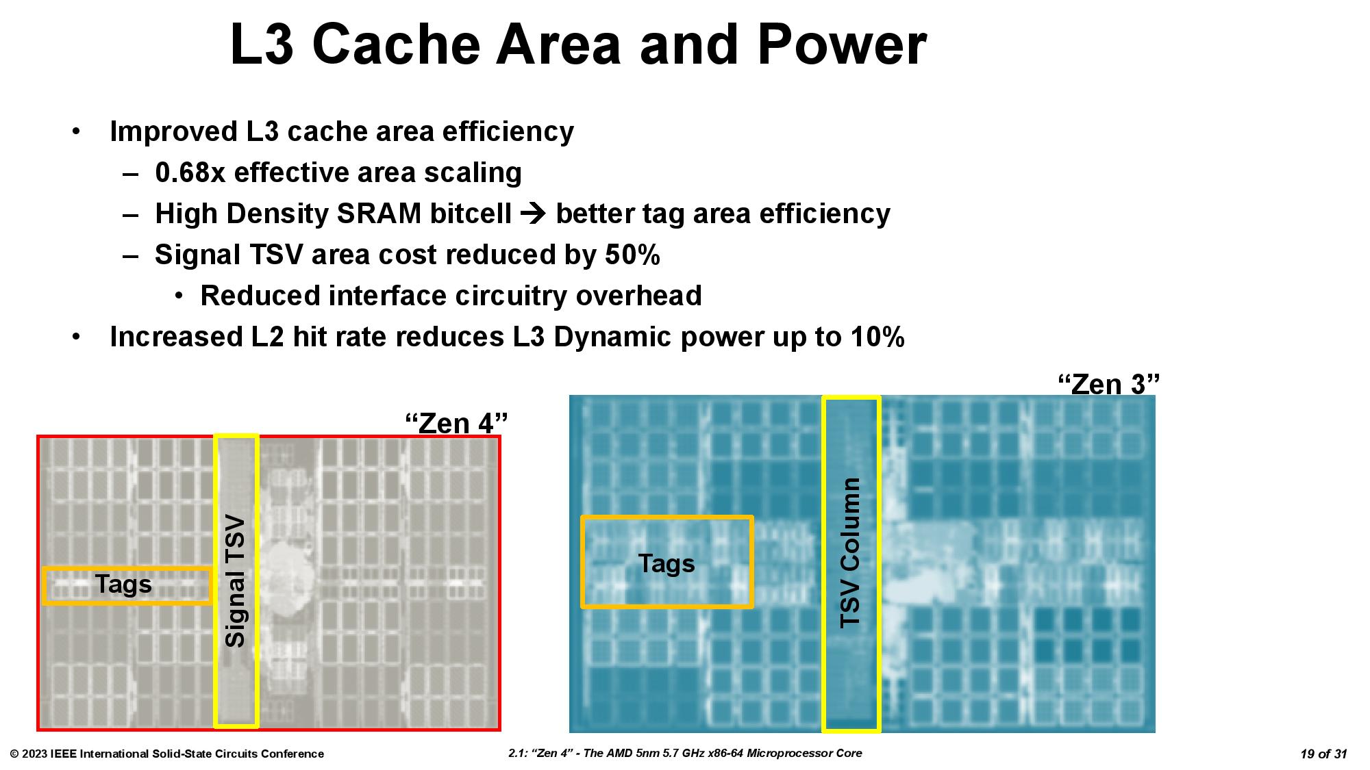
The stacked L3 SRAM chiplet is connected to the base die with two types of through-silicon vias (TSVs — a vertical electrical connection). The Power TSVs carry power between the chiplets, while the Signal TSVs carry data between the units.
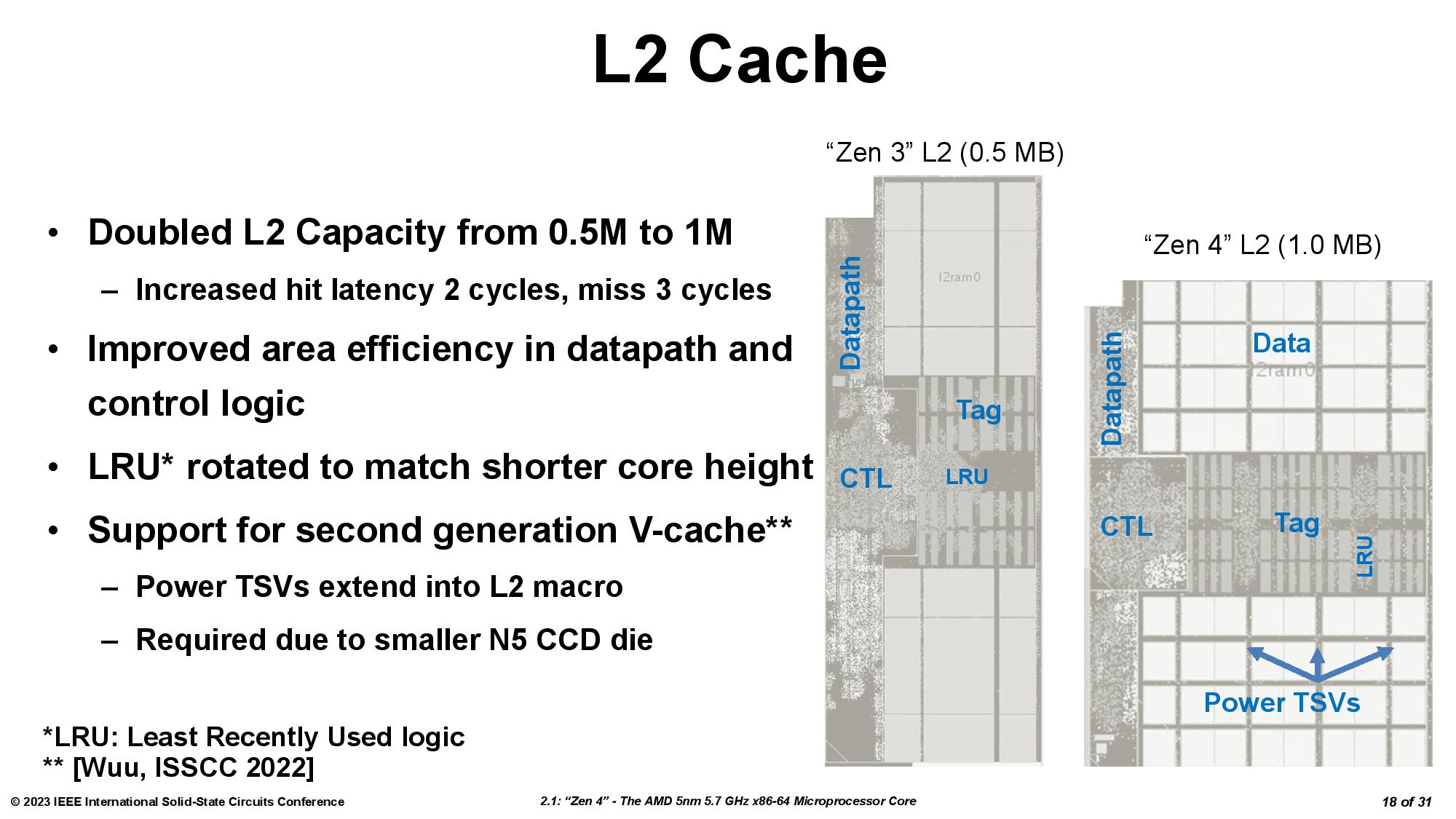
In the first-gen design, both types of TSVs resided in the L3 region of the base chiplet. However, the L3 cache on the base die is now smaller due to the increased density of the 5nm process, and even though the 7nm L3 SRAM chiplet is smaller, it now overlaps the L2 cache (the prior gen only overlapped the L3 on the base die). As such, AMD had to alter the TSV connections in both the base die and the L3 SRAM chiplet.


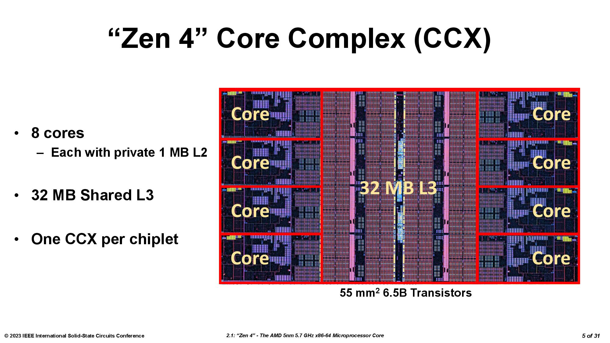
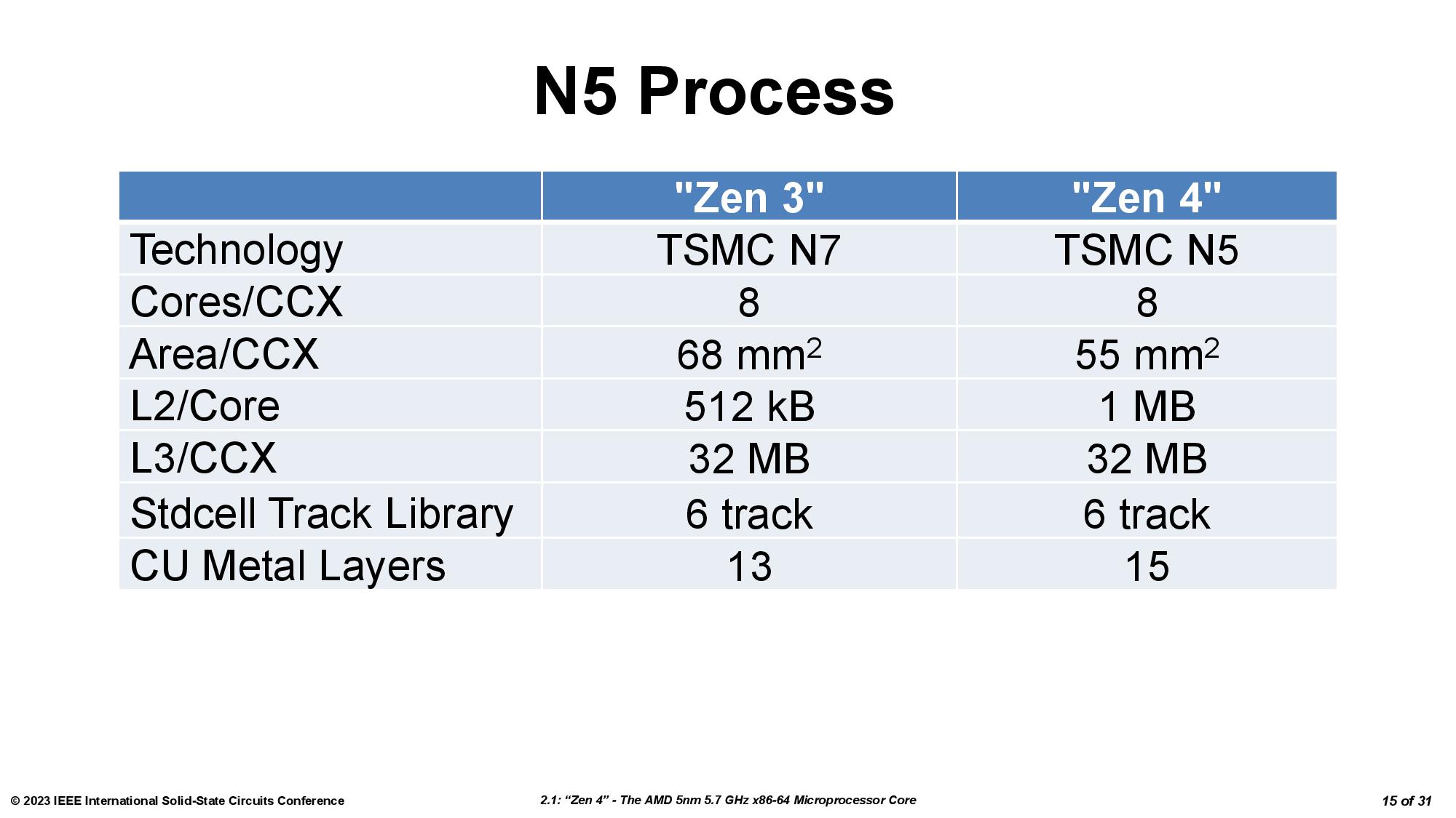

AMD had to extend the power TSVs from L3 into the L2 region due to the smaller size of the 5nm L3 cache on the base die (a result of the increased density and other factors). For the base die, AMD achieved a 0.68x effective area scaling across the L3 cache, data paths, and control logic compared to the old 7nm base chiplet, so there is physically less room for TSVs in the L3 cache.
The signal TSVs remain inside the L3 cache area on the base die, but AMD shrunk the TSV area in the L3 cache by 50% by applying learnings from the first-gen design along with DTCO improvements to reduce overhead circuitry in the new interface design.
AMD's 3D chip stacking tech is based on TSMC's SoIC technology. TSMC's SoIC is bump-less, meaning it doesn't use microbumps or solder to connect the two dies. You can read much more about the hybrid bonding and manufacturing process here. AMD tells us it used the same fundamental bonding process paired with continued process and DTCO improvements, but the minimum TSV pitch hasn't changed.
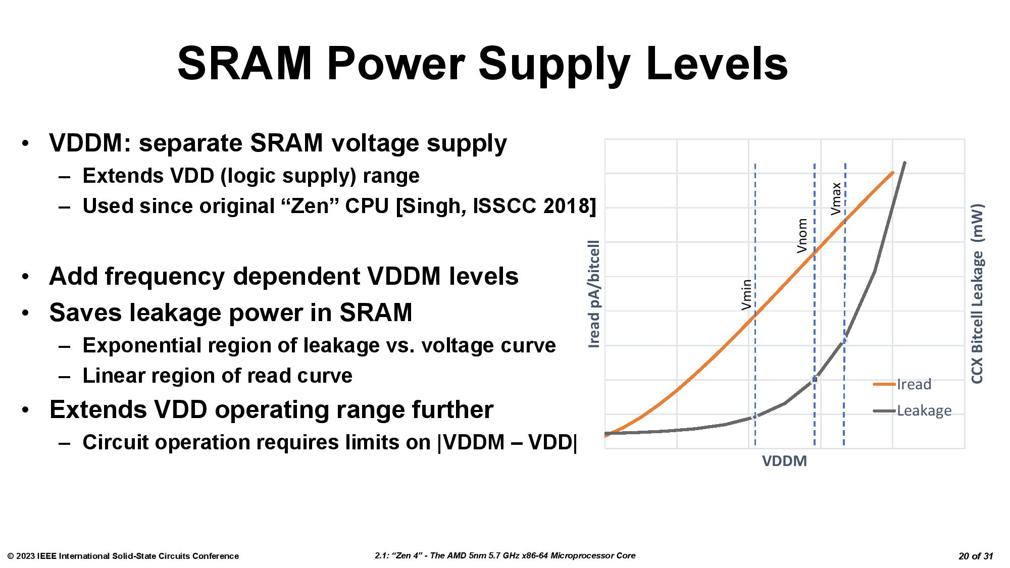
The L3 SRAM chiplet also remains on the same power domain as the CPU cores, so they can't be adjusted independently. This contributes to the lower frequency on the cache-equipped chiplet because the voltage can't exceed ~1.15V. You can see far more on that topic on the next page, where we test the chiplets individually.
Second-Gen 3D V-Cache L3 Latency and Bandwidth Testing
We tested each eight-core CCD separately to measure latency for both the chiplet with the 3D V-Cache (labeled as CCD 0 X3D), and the standard chiplet with the normal amount of L3 cache (CCD 1).
As before, the extra latency from the additional L3 SRAM cache weighs in at 4 clocks, but the bandwidth between the L3 chiplet and the base die has increased to 2.5 TB/s, a 25% improvement over the previous 2 TB/s peak.
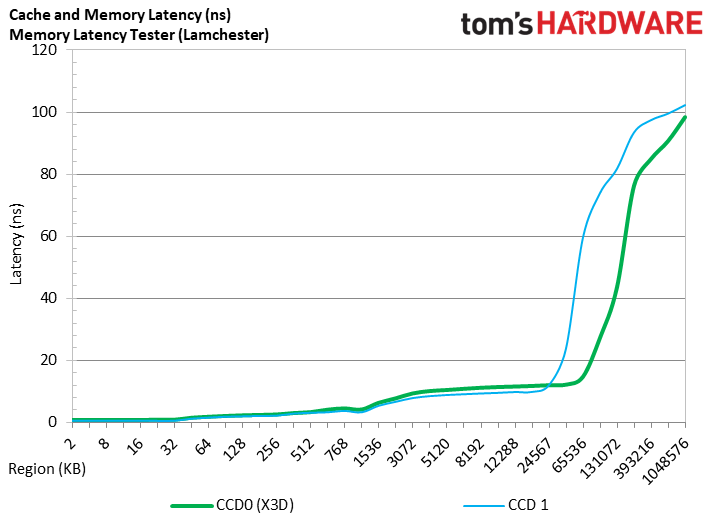
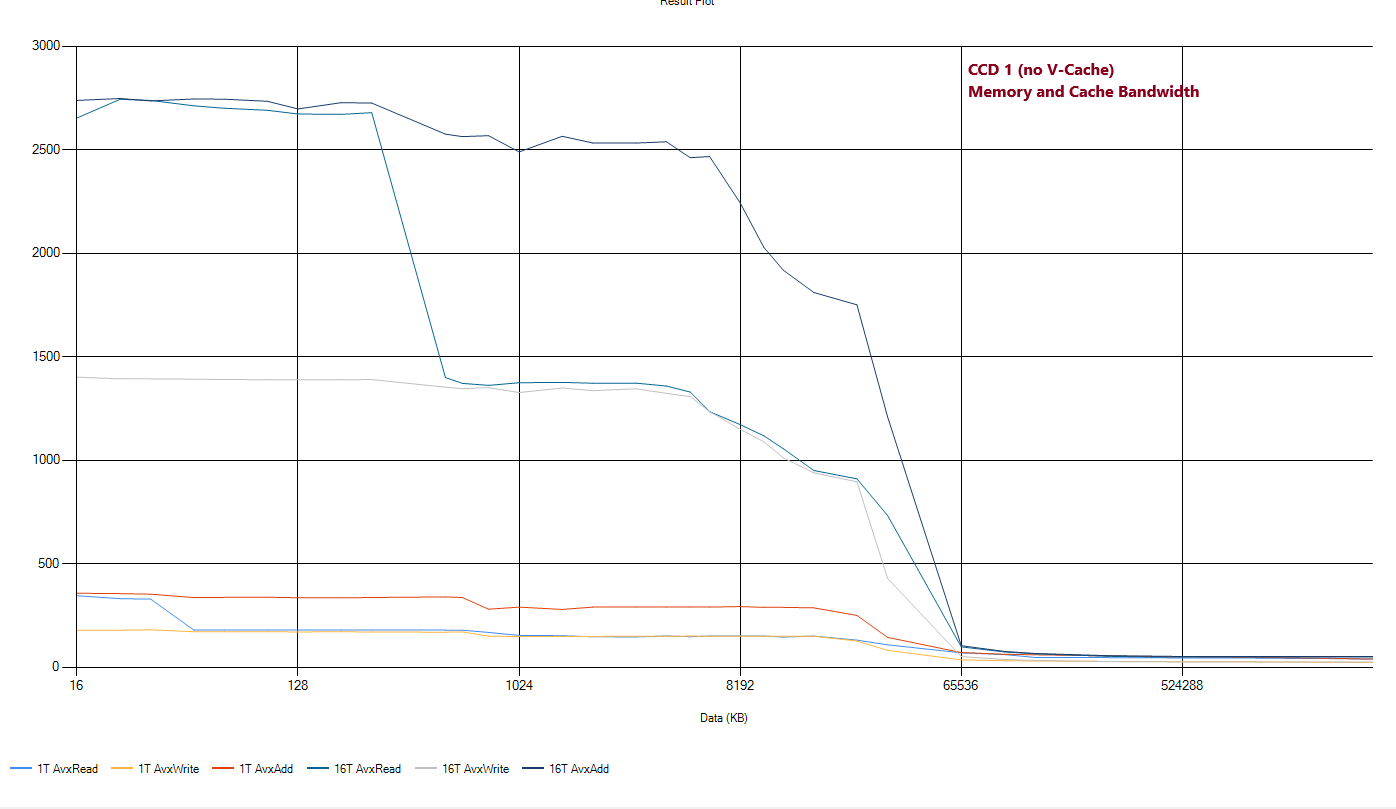
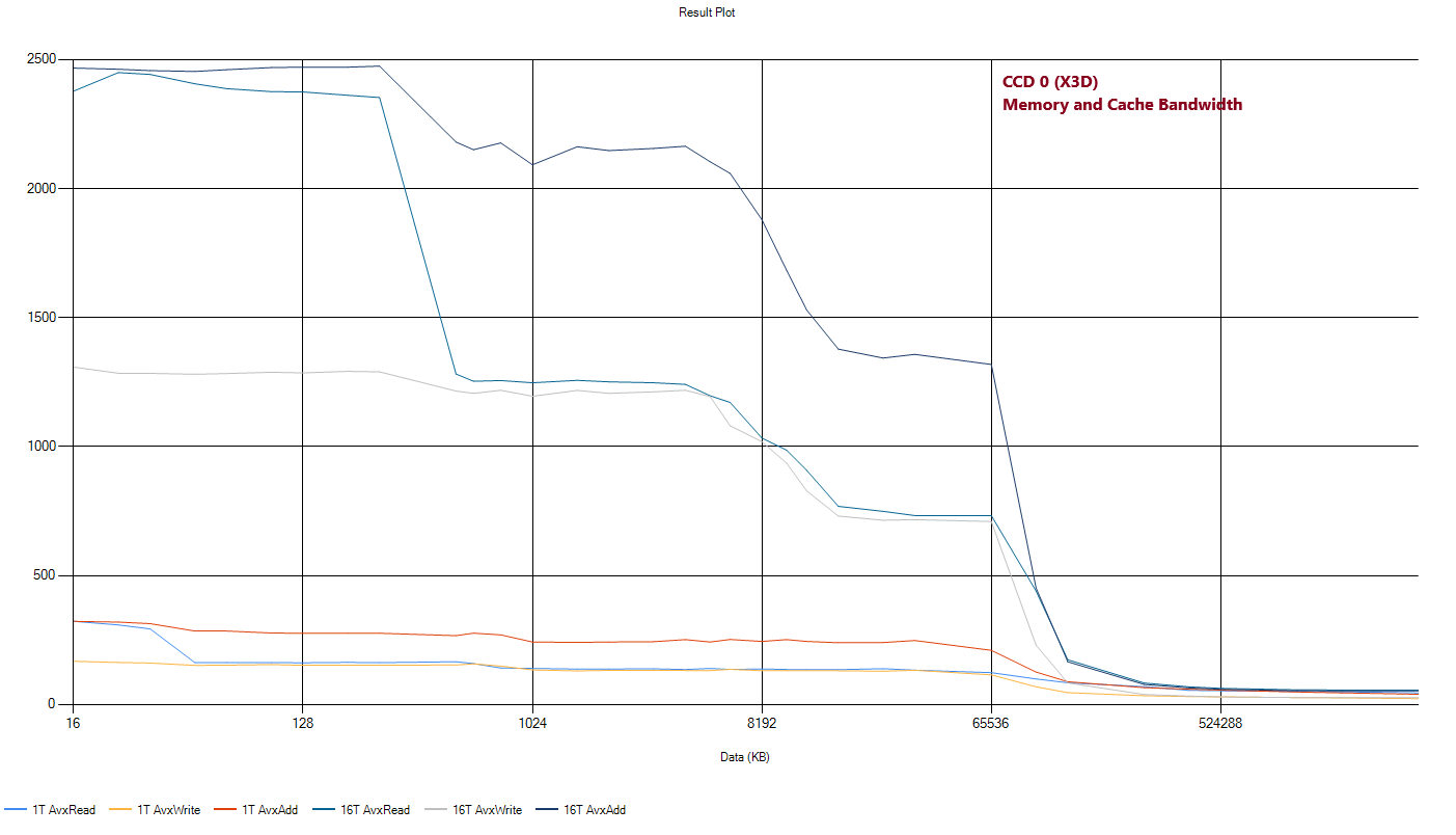
The album above outlines our cache and memory latency benchmarks with the Ryzen 9 7950X3D CCDs using the MemoryLatencyTool and MemoryBandwidthTest from the Chips and Cheese team. These tests measure cache latency and bandwidth varying sizes of data chunks.
Get Tom's Hardware's best news and in-depth reviews, straight to your inbox.
The tool measures the L3 latency for the 3D V-Cache equipped chiplet (CCD 0) on the Ryzen 7 5950X3D at 10-12ns, whereas the chiplet without the extra cache (CCD1) measures at 9ns. The higher latency comes from the additional cache capacity infused in the chiplet but is fairly small given the performance uplift you’ll see in the gaming benchmarks.
6nm I/O Die (IOD) for Zen 4 Ryzen 7000 and EPYC Genoa
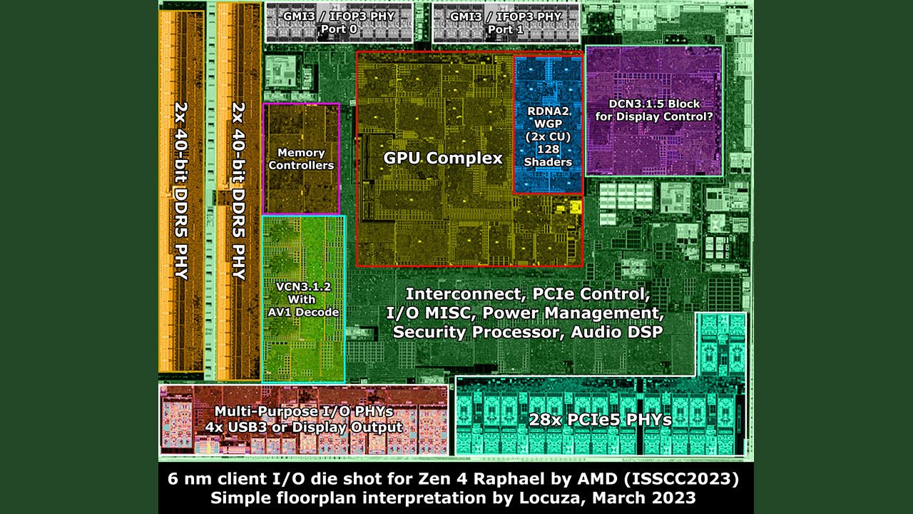
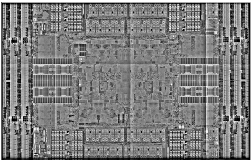
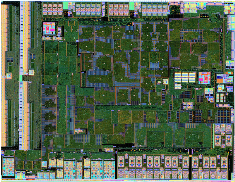
| Row 0 - Cell 0 | 6nm I/O Die (IOD) - Ryzen 7000 | 12nm I/O Die (IOD) - Ryzen 5000 | 6nm I/O Die (IOD) - EPYC |
| Size | 117.8mm^2 | 125mm^2 | 386.88mm^2 |
| Transistor Count | 3.37 Billion | 2.09 Billion | 11 billion |
| MTr/mm^2 (Transistor Density) | ~28.6 Million | ~16.7 Million | ~29.8 Million |
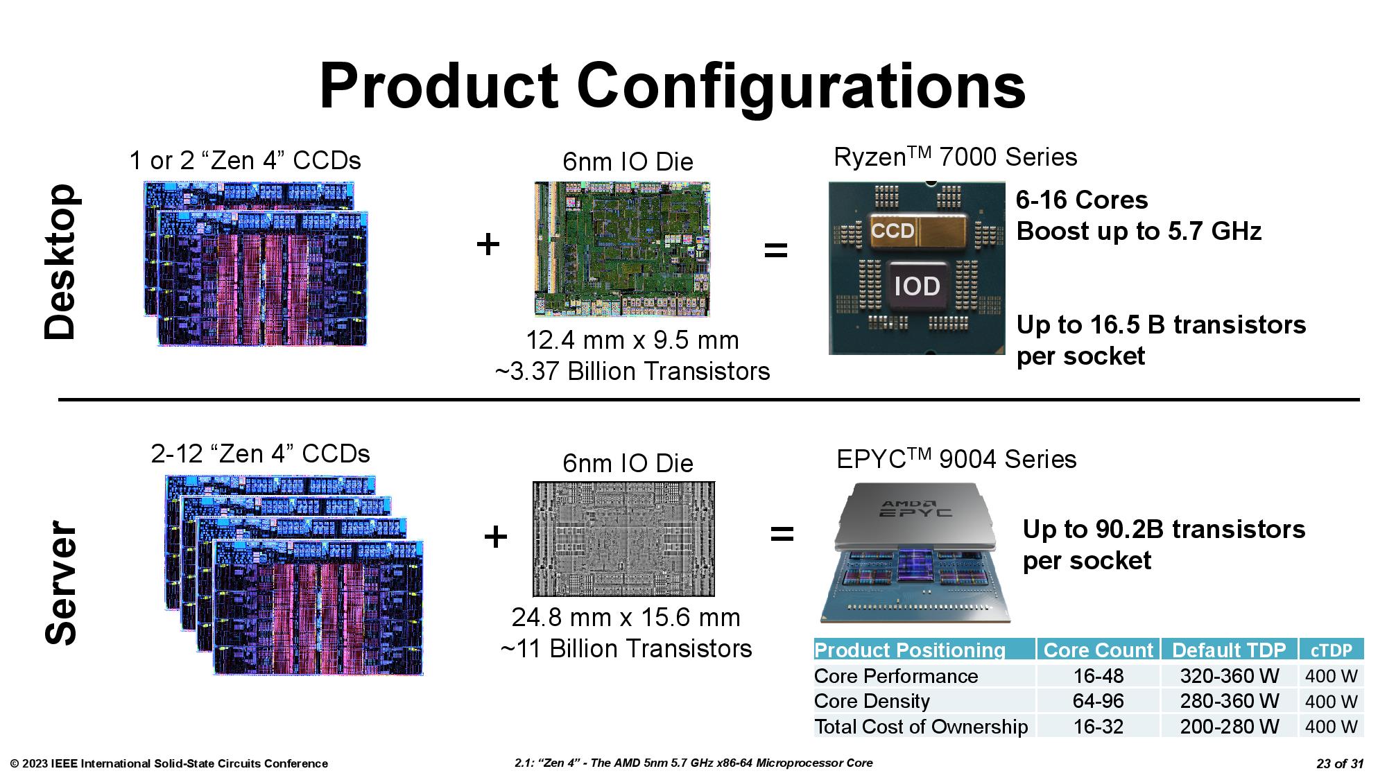
AMD's ISSCC presentation also included plenty of new details about the 6nm I/O Dies (IOD) used in the Ryzen 7000 and EPYC Genoa processors. In the above album, you can see the zoomed-in images and an annotated die shot from chip detective @Locuza_.
We put the specs in the table for easy comparison, and as you can see, the EPYC Genoa I/O Die is simply massive compared to the Ryzen 7000 variant — that's because AMD can wire up to 12 compute chiplets (CCDs) to the I/O Die for its EPYC Genoa processors.
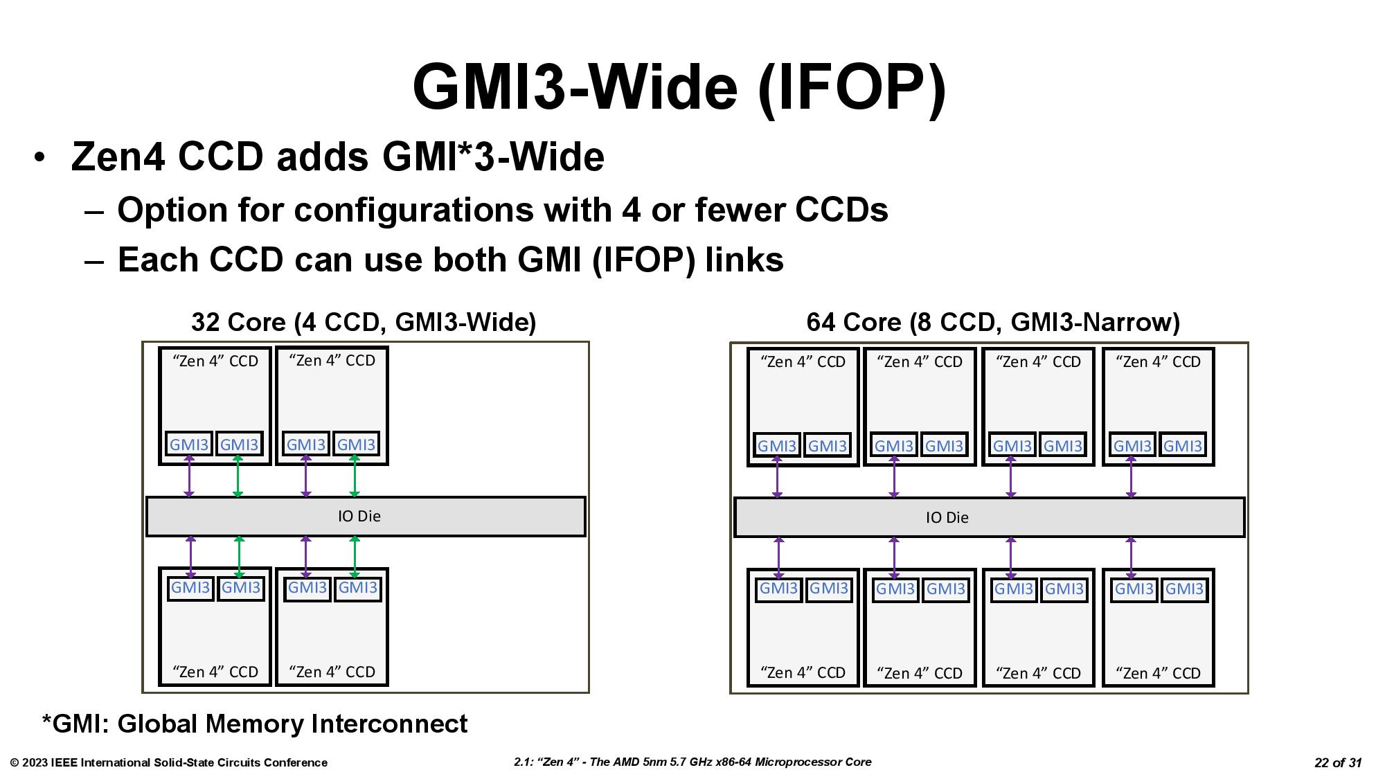
In contrast, the consumer chips are limited to two chiplets, an immutable limitation because, as you can see in the diagram, the Ryzen 7000 I/O Die only has two Global Memory Interconnect 2 (GMI2) links that connect the compute chiplets to the IOD. That's a bummer — the lower core-count Genoa models with four CCDs can have dual-GMI3 links (wide mode), a new capability that can offer advantages in some memory throughput-intensive tasks. That would've been interesting to add to the consumer chips. This limitation also rules out any three-CCD variants with this IOD.






- MORE: Best CPU for gaming
- MORE: CPU Benchmark Hierarchy
- MORE: Intel vs AMD
- MORE: How to Overclock a CPU
Current page: AMD Ryzen 9 7950X3D: 2nd-Gen 3D V-Cache Tech, Latency Testing
Prev Page 3D V-Cache For The High End Next Page 7950X3D Chiplet Boosts, Voltage, Thermal, and Throttling Tests
Paul Alcorn is the Editor-in-Chief for Tom's Hardware US. He also writes news and reviews on CPUs, storage, and enterprise hardware.
-
PlaneInTheSky ReplySteep pricing
The cons just weigh too heavy for me to even consider the CPU or the AM5 platform.
No support for DDR4 memory
Reduced performance in some productivity apps
I already have DDR4. AMD expects me to just throw this into the trash and buy expensive new DDR5 for a 1% difference in performance. It even bothers me from an e-waste perspective, let alone the financial cost.
The fact performance of X3D CPU is all over the place bothers me too. Yes it's fast in -some- games, but then you get less overall performance in several important applications. If I just used my PC for gaming, I would have bought a console, I don't like the idea of having to make a trade-off with X3D CPU.
Another thing is, and this is not AMD specific but PC specific. The biggest issue with gaming on PC has been stuttering because shaders need to be runtime compiled on PC. This CPU will not solve this. When PC gaming becomes a meme, #stutterstruggle, I don't think many people are going to be willing to invest in $600+ CPU. Solve this problem, PC gaming is currently in shambles. -
cknobman Every single media outlet beating the "DDR5 cost" dead horse over and over again.Reply
When talking about ultimate gaming performance, which these 3D chips are designed for, saying the platform cost of DDR5 is a negative is stupid.
DDR4 is a dead end and should only be considered for budget builds and upgrades on older systems at this point.
Just let the "platform cost" argument go, otherwise test Intel with DDR4 and make proper comparisons showing what you get going with older and slower technology. -
PEnns Wow, AMD is for once forcing users to upgrade to new hardware.......and DDR5! How horrible!!Reply
I heard that lame story so many times before, Intel does it every 2-3 years!!! -
drivinfast247 Reply
I don't think they're targeting you specifically. No need to upgrade if not needed. Don't forget there's other people whom may be building their first PC or upgrading from a very old platform and the performance increase will be astronomical.PlaneInTheSky said:The cons just weigh too heavy for me to even consider the CPU or the AM5 platform.
I already have DDR4. AMD expects me to just throw this into the trash and buy expensive new DDR5 for a 1% difference in performance. It even bothers me from an e-waste perspective, let alone the financial cost.
The fact performance of X3D CPU is all over the place bothers me too. Yes it's fast in -some- games, but then you get less overall performance in several important applications. If I just used my PC for gaming, I would have bought a console, I don't like the idea of having to make a trade-off with X3D CPU.
Another thing is, and this is not AMD specific but PC specific. The biggest issue with gaming on PC has been stuttering because shaders need to be runtime compiled on PC. This CPU will not solve this. When PC gaming becomes a meme, #stutterstruggle, I don't think many people are going to be willing to invest in $600+ CPU. Solve this problem, PC gaming is currently in shambles.
Curious as to what games are struggling to run on PC and also what PCs are struggling to run games? Also, are those affected games also having issues on consoles?
My PC runs every game that I play without issues. And with the recent GPU upgrade I'll be happy for another year or so and will upgrade when needed. -
Elusive Ruse Reply
Ah cut the crap will you?PlaneInTheSky said:The cons just weigh too heavy for me to even consider the CPU or the AM5 platform.
I already have DDR4. AMD expects me to just throw this into the trash and buy expensive new DDR5 for a 1% difference in performance. It even bothers me from an e-waste perspective, let alone the financial cost.
The fact performance of X3D CPU is all over the place bothers me too. Yes it's fast in -some- games, but then you get less overall performance in several important applications. If I just used my PC for gaming, I would have bought a console, I don't like the idea of having to make a trade-off with X3D CPU.
Another thing is, and this is not AMD specific but PC specific. The biggest issue with gaming on PC has been stuttering because shaders need to be runtime compiled on PC. This CPU will not solve this. When PC gaming becomes a meme, #stutterstruggle, I don't think many people are going to be willing to invest in $600+ CPU. Solve this problem, PC gaming is currently in shambles.
You have no intention of upgrading to anything, you have admitted it before. All you do here is dump on new tech because for some reason you cannot deal with change. You have an axe to grind when it comes to AMD and anything that puts your fossil of a setup into perspective.PlaneInTheSky said:My PC from 14 years ago still browses the internet just fine. It still does Spotify, Netflix, indie gaming, etc.
At some point your average PC became "good enough" for most tasks.
This is starting to happen with PC gaming too. While AAA developers still bother to spend years making "uber graphics", most developers have long stopped with this rat race because better graphics rarely translates to better sales.
-
Elusive Ruse Reply
Especially considering that Intel's 13th gen would take a massive performance plunge if paired with DDR4.cknobman said:Every single media outlet beating the "DDR5 cost" dead horse over and over again.
When talking about ultimate gaming performance, which these 3D chips are designed for, saying the platform cost of DDR5 is a negative is stupid.
DDR4 is a dead end and should only be considered for budget builds and upgrades on older systems at this point.
Just let the "platform cost" argument go, otherwise test Intel with DDR4 and make proper comparisons showing what you get going with older and slower technology.
It is intellectually disingenuous to put lack of DDR4 support as a con here, if only for the reason that it has already been established that AM5 doesn't support it. Is Tom's Hardware going to put "Lack of DDR4 support" as a con for every CPU that comes out from now on? -
lmcnabney Excellent article.Reply
I noted that Paul mentioned AMD's specification to use water-cooling on the X3D lineup. After noting the low power usage of these chips I am curious as to why. Has the chip been tested using a more typical air cooled tower fan (with both standard, PBO, and PBO-UV) to determine if water-cooling is even necessary? -
Elusive Ruse Reply
According to AMD, V-cache is sensitive to heat; that's why they decreased the TjMax to 89c and reduced the TDP as well. I assume that's also why they instructed reviewers to use water-cooling.lmcnabney said:Excellent article.
I noted that Paul mentioned AMD's specification to use water-cooling on the X3D lineup. After noting the low power usage of these chips I am curious as to why. Has the chip been tested using a more typical air cooled tower fan (with both standard, PBO, and PBO-UV) to determine if water-cooling is even necessary? -
Alvar "Miles" Udell 13% faster in games at 1920x1080 comparing stock to stock for 20% more money (or 25% if using the current discount)...that's proper gamer logic for sure.Reply
If anything it's an advertisement for the 5800x3d. 16% slower at 1920x1080 yet only 44% of the price, plus the platform cost is far cheaper and all you sacrifice is PCIe 5.0.
