GeForce GTX 480 And 470: From Fermi And GF100 To Actual Cards!
Get Tom's Hardware's best news and in-depth reviews, straight to your inbox.
You are now subscribed
Your newsletter sign-up was successful
Additional Reading: Memory Hierarchy, Setup Engine, Tessellation
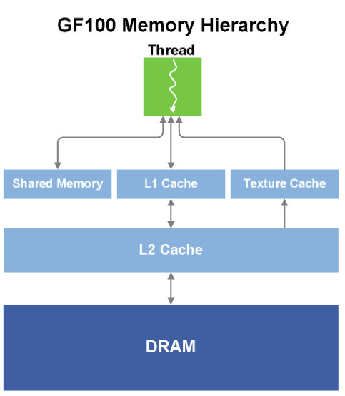
A Memory Hierarchy Worthy Of A CPU
For a long time, the memory subsystem was the GPU’s “red-headed stepchild.” Admittedly, memory access with early GPUs was so simple that a memory hierarchy wasn’t really needed. A simple texture cache and a small vertex cache (pre- and post-transformation) were all it took. With the arrival of GPGPU, things have become more complex, and a memory subsystem that basic isn't enough.
To meet these new requirements, Nvidia introduced Shared Memory with the G80. Shared Memory is a small, extremely-fast memory area built into each multiprocessor that enables data sharing among threads. Even though using this memory area was totally the responsibility of the programmer (and consequently required additional effort), the concept was well-received and reappeared in subsequent AMD GPUs. Finally, Microsoft integrated it into Direct3D 11, and Khronos into OpenCL.
But while this kind of memory, managed manually by the programmer, offers excellent performance with algorithms where memory access is highly predictable, it can’t supplant a cache when memory accesses are irregular. With GF100, Nvidia tried to combine the best of both worlds by offering a 64KB memory area per multiprocessor. This memory area can be configured in two different ways:
- 16KB of L1 cache and 48KB of Shared Memory
- 48KB of L1 cache and 16KB of Shared Memory
This L1 cache can be used as a buffer to back up the registers when space is short, which is not a bad thing. While their number has increased compared to GT200, the increase isn’t commensurate with the increase in the number of stream processors.
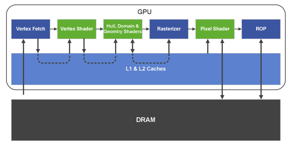
But that’s not all. As we saw earlier, Nvidia also adds a true L2 cache to the GPU. GT200 did have a 256KB L2, but it was accessible only for reading, and only by the texture units. With GF100, Nvidia gives its GPU a general-purpose L2 cache--that is, accessible in read/write mode--for texture instructions and for load/store instructions. This cache also replaces the ROP cache and the pre- and post-vertex transform cache of preceding GPUs. The L1 texture cache, due to its somewhat special functioning, is still present and is the same size as on GT200 (12KB).
Finally, A Parallelized Setup Engine!
Get Tom's Hardware's best news and in-depth reviews, straight to your inbox.
The benchmark of one triangle generated per clock cycle has finally been surpassed! We’ve been waiting for it for a long time (since the arrival of unified architectures, in fact), representing a great leap forward in geometry power. For a short while, we even thought that RV870 had paved the way, but that was an unfortunate letdown. But now Nvidia is stepping up by multiplying the number of setup units, and it's being generous. There are not two, but four rasterizers!
Here’s where the new organization of the units shows its full potential. As we said, each GPC contains most of the functions of a GPU (except for the ROP units), and can consequently function independently. What that means is that each GPC has its own setup unit, which can rasterize one triangle per cycle (at 8 pixels per cycle). In practice, the peak performance is unchanged: 32 pixels are still generated per cycle, as with GT200 and RV870, but the effectiveness of the new architecture will be evident when numerous small triangles are being handled.
Like most tech companies, Nvidia has a marketing department that's always eager to come up with exotic names for familiar concepts, so it includes all of the operations performed on vertices within a GPC using the PolyMorph Engine moniker.
The geometric pipeline is as follows: the vertices are taken from a buffer, then passed to the multiprocessors, which perform the vertex shading. The result is then passed on to the next stage of the PolyMorph Engine (the Tesselator), which is not directly programmable, but whose operation can be controlled by the Hull Shader, upstream, and the Domain Shader, downstream on the multiprocessors.
Tessellation
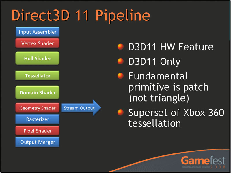
A little review of tessellation is appropriate here. In Direct3D 11, Microsoft introduced three new stages to its graphics pipeline (in green in the illustration): the Hull Shader, the Tessellator, and the Domain Shader. Unlike the other stages in the pipeline, they don’t operate with triangles as primitives, but with patches. The Hull receives the control points of a patch as input, determines certain parameters of the Tessellator (for example, the TessFactor, which indicates the degree of tessellation). The Tessellator is a fixed-function unit, and consequently the programmer doesn’t control how the tessellation is performed; it sends the points it generates to the Domain Shader, which can apply operations to them.
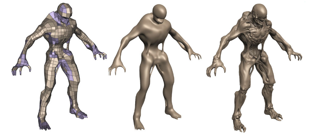
Tessellation has multiple advantages. It enables very compact storage of geometric data. Only the control points of the mesh are stored in memory, and the additional vertices generated remain in the graphics pipeline, which saves memory and bandwidth. Another advantage is that tessellation enables the use of dynamic LOD (levels of detail). The closer a mesh is to the camera, the more detailed it needs to be. Conversely, if it’s farther away, using a huge number of triangles is not only superfluous, but it can also be a huge drag on performance since the rasterizers and shader units aren’t at ease with triangles that are too small.
Tessellation also has advantages in terms of animation; animation data is necessary only for the control points (the "coarse" mesh, in simple terms), whereas on a very complex mesh, it should be be available for each vertex. Consequently, the gains at this level can be used by adding more animation data per control point, improving the quality of the animation.
But let’s be clear: while Microsoft, AMD, and Nvidia try to make the situation sound idyllic, in practice, tessellation is not a magic wand that automatically increases a game's level of geometric detail. Implementing tessellation properly in an engine is still complex and requires work to avoid the appearance of visual artifacts, especially at the intersections between two surfaces with different tessellation factors.
For an analysis of tessellation performance, check out this page earlier in our review.
Current page: Additional Reading: Memory Hierarchy, Setup Engine, Tessellation
Prev Page Additional Reading: SMs, Scheduler, And Texturing Next Page Additional Reading: Geometry, Raster, ROP, And GPGPU-
restatement3dofted I have been waiting for this review since freaking January. Tom's Hardware, I love you.Reply
With official reviews available, the GTX 480 certainly doesn't seem like the rampaging ATI-killer they boasted it would be, especially six months after ATI started rolling out 5xxx cards. Now I suppose I'll just cross my fingers that this causes prices for the 5xxx cards to shift a bit (a guy can dream, can't he?), and wait to see what ATI rolls out next. Unless something drastic happens, I don't see myself choosing a GF100 card over an ATI alternative, at least not for this generation of GPUs. -
tipoo Completely unimpressed. 6 months late. Too expensive. Power hog. Performance not particularly impressive. The Radeon 5k series has been delivering a near identical experience for 6 months now, at a lower price.Reply
-
tpi2007 hmmm.. so this is a paper launch... six months after and they do a paper launch on a friday evening, after the stock exchange has closed.. smart move by Nvidia, that way people will cool off during the weekend, but I think their stocks won't perform that brilliantly on monday...Reply -
Godhatesusall high power consumption, high prices along with a (small, all things considered) performance edge over ATI is all there is. Are 100$ more for a gtx 480 really worth 5-10% increase in performance?Reply
Though the big downside of fermi are temps. 97 is a very large(and totally unacceptable) temperature level. IMO fermi cards will start dying from thermal death some months from now.
I just wanted competition,so that prices would be lower and we(the consumers) could get more bang for our buck. Surely fermi doesnt help alot in that direction(a modest 30$ cut for 5870 and 5850 from ATI and fermi wont stand a chance). It seems AMD/ATI clearly won this round -
Pei-chen Wow, it seems Nvidia actually went ahead and designed a DX11 card and found out how difficult it is to design. ATI/AMD just slapped a DX11 sticker on their DX10 card and sells it as DX11. In half a year HD 5000 will be so outdated that all it can play is DX10 games.Reply -
outlw6669 Kinda impressed :/Reply
The minimum frame rates are quite nice at least...
Lets talk again when a version with the full 512 SP is released.


