GeForce GTX 480 And 470: From Fermi And GF100 To Actual Cards!
Nvidia’s GF100 Gets Scaled Back
We presented the GF100 GPU, based on Nvidia’s Fermi architecture, back in January. At the time, we forecasted the potential for a 2x performance boost transitioning from GT200-based cards like the GeForce GTX 285 to a GF100-based flagship. Of course, that was also based on the assumption we’d be seeing graphics cards equipped with the complete GF100. As it turns out, that isn’t the case.
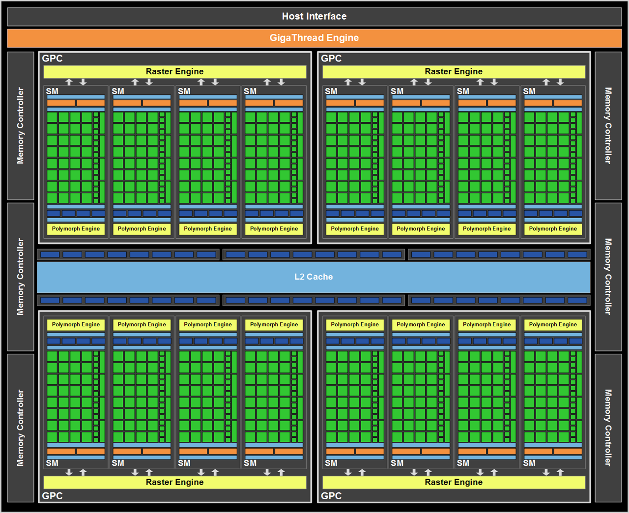
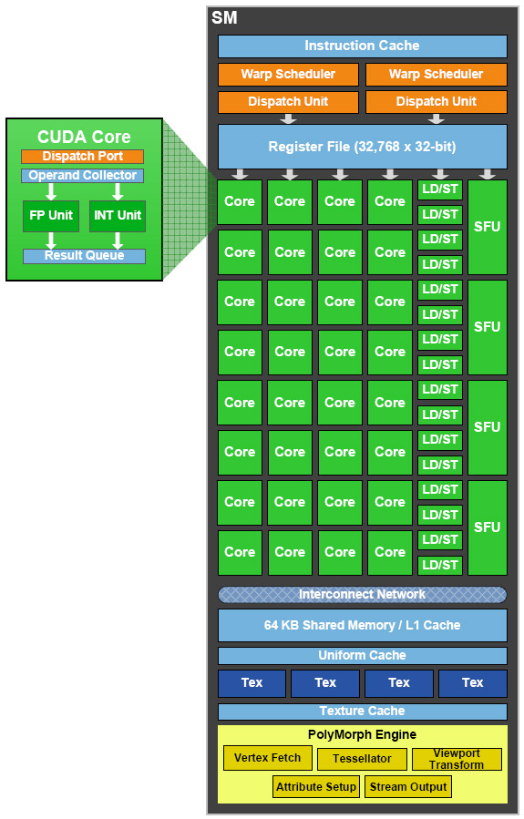
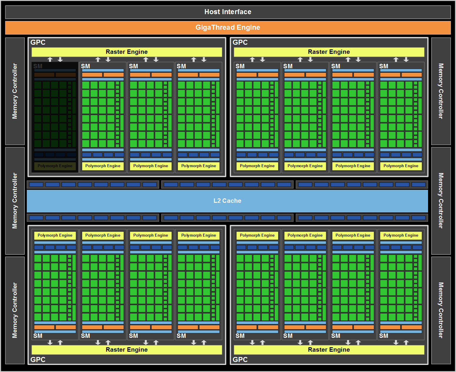
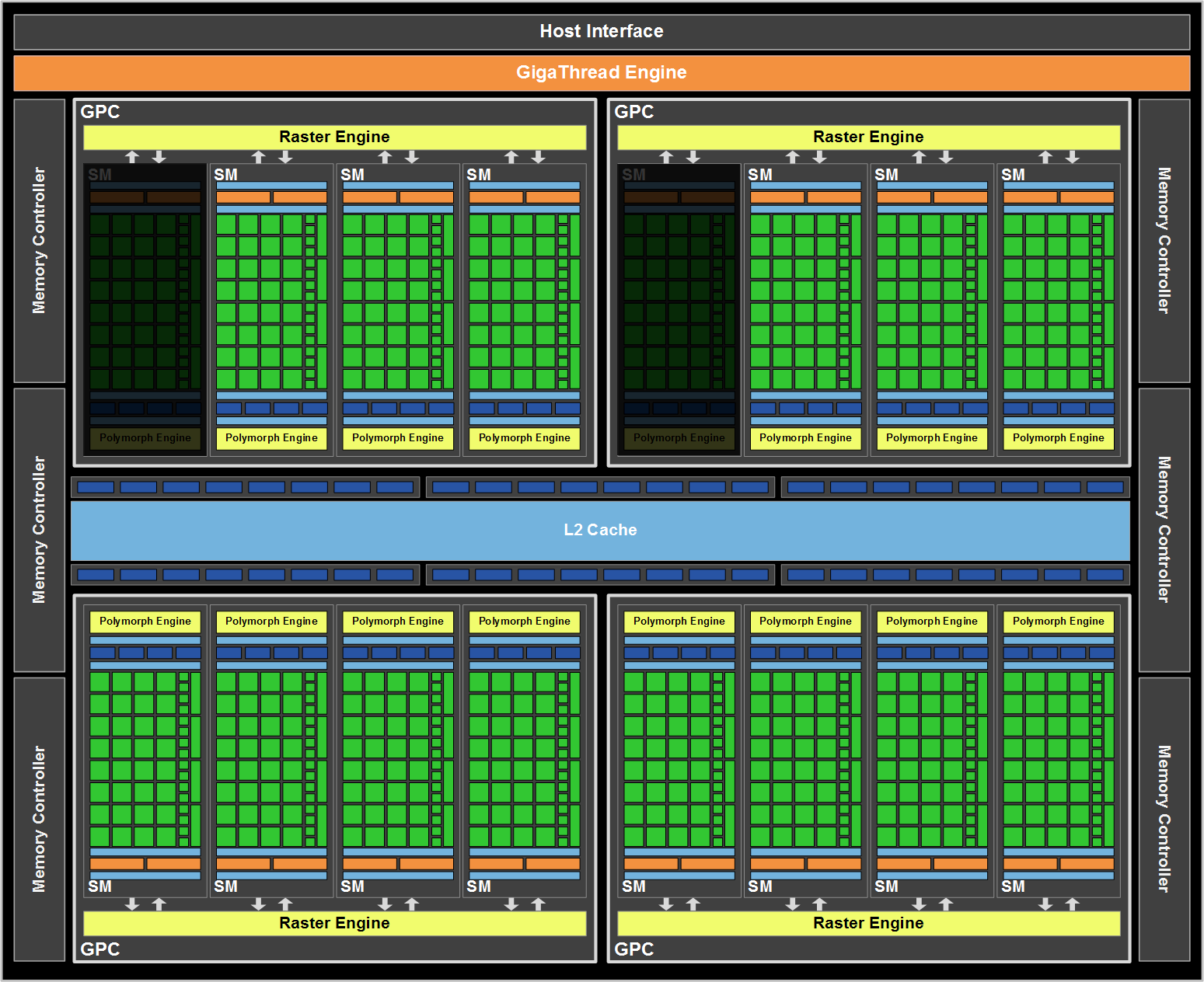
In its full form, the three billion transistor GF100 features 512 CUDA cores (derived from four Graphics Processing Clusters [GPCs], each with four Streaming Multiprocessors [SMs], and each of those sporting 32 CUDA cores). But the GeForce GTX 480 employs 480 CUDA cores, while the GTX 470 is armed with 448—32-core drops in each case. Nvidia achieves this by disabling one of the GTX 480’s SMs and two of the GTX 470’s.
Because each SM also contains its own texture units and PolyMorph engine (the fixed-function logic responsible for the architecture’s exceptional geometry performance), both new cards sacrifice performance in those two areas, as well. The GeForce GTX 480 retains 60 texture units (down from 64) and 15 PolyMorph engines, while the GeForce GTX 470 offers 56 texture units and 14 PolyMorph engines.
GF100’s back-end is of course independent of the GPCs, so even with its scaled-back GeForce GTX 480 configuration, Nvidia is able to maintain all six ROP partitions. Each partition is capable of outputting eight 32-bit integer pixels at a time, totaling 48 pixels per clock. The GeForce GTX 470 isn’t as lucky; it loses one of the ROP partitions (dropping total pixels per clock to 40).
A complete GF100, with all of its ROP partitions intact, sports a 384-bit GDDR5 memory interface (one 64-bit interface per partition). The GeForce GTX 480 comes to the table with this exact configuration, serving up 256MB per interface for a total of 1.5GB of GDDR5 memory (that’s 177 GB/s, when you take the 924 MHz clock rate into account). Naturally, the GeForce GTX 470 gives some of that up. Its 320-bit interface plays host to 1.25GB of GDDR5 at a lower 837 MHz clock rate, which adds up to nearly 134 GB/s.
So there you have it. We’re looking at the same graphics processor presented back in January. As a result of yield issues, however, Nvidia’s new flagship and second-in-command are forced to employ a scaled-back version of the chip. While we’re certainly not expecting to multiply the performance of GeForce GTX 285 anymore, these should still compete aggressively with AMD’s Radeon HD 5870 and 5850 cards. Speaking of cards…
Get Tom's Hardware's best news and in-depth reviews, straight to your inbox.
Current page: Nvidia’s GF100 Gets Scaled Back
Prev Page The Way It’s Meant To Be Played? Next Page Meet The GeForce GTX 480 And 470-
restatement3dofted I have been waiting for this review since freaking January. Tom's Hardware, I love you.Reply
With official reviews available, the GTX 480 certainly doesn't seem like the rampaging ATI-killer they boasted it would be, especially six months after ATI started rolling out 5xxx cards. Now I suppose I'll just cross my fingers that this causes prices for the 5xxx cards to shift a bit (a guy can dream, can't he?), and wait to see what ATI rolls out next. Unless something drastic happens, I don't see myself choosing a GF100 card over an ATI alternative, at least not for this generation of GPUs. -
tipoo Completely unimpressed. 6 months late. Too expensive. Power hog. Performance not particularly impressive. The Radeon 5k series has been delivering a near identical experience for 6 months now, at a lower price.Reply
-
tpi2007 hmmm.. so this is a paper launch... six months after and they do a paper launch on a friday evening, after the stock exchange has closed.. smart move by Nvidia, that way people will cool off during the weekend, but I think their stocks won't perform that brilliantly on monday...Reply -
Godhatesusall high power consumption, high prices along with a (small, all things considered) performance edge over ATI is all there is. Are 100$ more for a gtx 480 really worth 5-10% increase in performance?Reply
Though the big downside of fermi are temps. 97 is a very large(and totally unacceptable) temperature level. IMO fermi cards will start dying from thermal death some months from now.
I just wanted competition,so that prices would be lower and we(the consumers) could get more bang for our buck. Surely fermi doesnt help alot in that direction(a modest 30$ cut for 5870 and 5850 from ATI and fermi wont stand a chance). It seems AMD/ATI clearly won this round -
Pei-chen Wow, it seems Nvidia actually went ahead and designed a DX11 card and found out how difficult it is to design. ATI/AMD just slapped a DX11 sticker on their DX10 card and sells it as DX11. In half a year HD 5000 will be so outdated that all it can play is DX10 games.Reply -
outlw6669 Kinda impressed :/Reply
The minimum frame rates are quite nice at least...
Lets talk again when a version with the full 512 SP is released.


