GeForce GTX 480 And 470: From Fermi And GF100 To Actual Cards!
Additional Reading: SMs, Scheduler, And Texturing
Whereas AMD was able to limit itself to a few minor revisions with Cypress, Nvidia needed to radically change the G80 architecture it introduced over three years ago. The organization of the various units has been completely reworked. GT200 employed what Nvidia called TPCs (Texture Processor Clusters), consisting of one texture unit and three Streaming Multiprocessors (SMs). Nvidia maintains the term Streaming Multiprocessor with the GF100, but these units are now much more powerful.
Streaming Multiprocessors
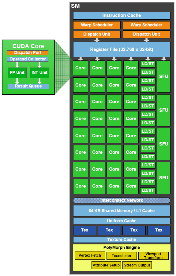
With GT200, a Streaming Multiprocessor was made up of one 8-way SIMD units, two special function units, and one double-precision unit. With GF100, they now have two 16-way SIMD units and four special function units. So, there is no longer an ALU specifically dedicated to double-precision. FP64 calculation is now carried out by the same units at half the rate.
The increase in processing power is not the most notable change; the texture units are now directly implemented in the SM, whereas beforehand they were decoupled (three SMs shared eight texture units). On GF100, each SM has four texture units of its own, which also explains why their overall number has decreased compared to the preceding architecture (eight units per TPC on GT200 [or a total of 80], compared to four units per SM on GF100 [or a total of 60 for the GTX 480]). Another new feature is the 16 load/store units, enabling addresses to be calculated in cache memory or in RAM for 16 threads per cycle.
Concretely, this reorganization allows Nvidia to offer a much more elegant and more effective architecture than the previous one. The SMs are really independent processors, whereas beforehand they relied on a memory subsystem shared by groups of three SMs.
The size of the register file has also increased. Instead of 16,384 32-bit registers per multiprocessor, there are now 32,768. At the same time, the number of active threads per multiprocessor has increased compared to the GT200, from 1,024 threads (24 warps of 32 threads) to 1,536 (48 warps of 32 threads). Thus, the number of registers available per thread is 21 compared to 16 beforehand (and 10 on G80). Now let’s test the increase in processing power using a few shaders.
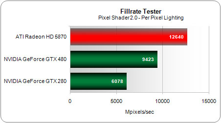
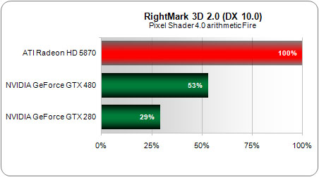
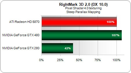
On a now-very-simple shader test, lighting per pixel in DirectX 9, the GeForce GTX 480 is 55% more efficient than the GeForce GTX 280. This increases to 82% with a heavier shader using procedural textures.
Get Tom's Hardware's best news and in-depth reviews, straight to your inbox.
Dual-Scheduler
Since the appearance of its G80 architecture, Nvidia has been saying that its multiprocessors are capable of executing two instructions per cycle in certain circumstances: one MUL and one MAD. We weren’t able to confirm that with the early versions of the design, and even on the GT200 it was especially difficult to demonstrate. In practice, the famous dual-issue Nvidia was talking up wasn’t observable; the chip could execute only one MAD per cycle.
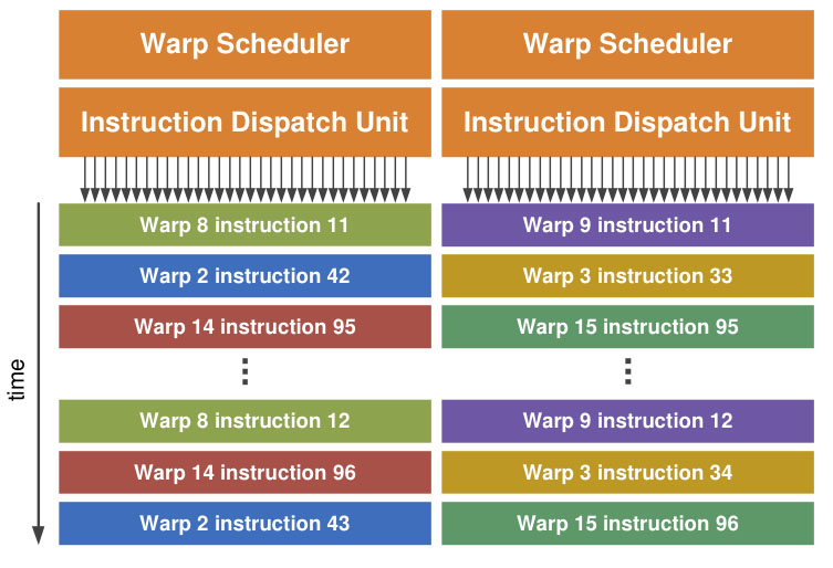
That’s not so important anymore because Nvidia’s GF100 has two schedulers that enable execution of two instructions per cycle without the constraints that limited previous architectures. As we saw earlier, the 32 stream processors in each multiprocessor are, in fact, arranged in two groups of 16 units, and each of these groups can execute one independent instruction. The recent history of CPUs has proven that superscalar execution is very complex to implement. But Nvidia has a major advantage in this area: GF100 doesn’t attempt to extract parallelism from a single instruction flow, with all the possibilities for error that implies. In fact, the multiprocessor selects two warps and launches execution of one instruction from each of them on the SIMD units. Since the warps are totally independent, they can be executed in parallel without any risk.
Most instructions, whether FP32 calculation instructions, integers, or load/store, can be executed simultaneously. The only exception to that rule is double-precision calculation instructions, which use all 32 stream processors and can’t be executed simultaneously with any other type of instruction.
Texture Units
Though the number of texture units has decreased, Nvidia has completely redesigned them in its current-generation architecture to improve performance. As we said, they are now built into the multiprocessors, which avoids having to share them among several multiprocessors, with all the loss of efficiency that involves. The L1 cache dedicated to texture units has also been redesigned, and though its size is unchanged from GT200 (12KB), Nvidia says that it’s much more efficient. Finally, the texture units are now clocked at the GPU frequency, whereas previously they operated at a lower frequency.
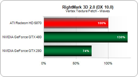
The result: on this test, which measures texture access performance (useful for displacement mapping, for example), the GeForce GTX 480 tested 75% more efficient than the GTX 280.
Obviously, the new units support the new BC6H and BC7H compression formats and the Gather instructions required by Direct3D 11. And performance with more contemporary pixel shaders has indeed increased, though that’s really a matter of catching up with the competition.
Current page: Additional Reading: SMs, Scheduler, And Texturing
Prev Page Additional Reading: Breaking Down GF100 Next Page Additional Reading: Memory Hierarchy, Setup Engine, Tessellation-
restatement3dofted I have been waiting for this review since freaking January. Tom's Hardware, I love you.Reply
With official reviews available, the GTX 480 certainly doesn't seem like the rampaging ATI-killer they boasted it would be, especially six months after ATI started rolling out 5xxx cards. Now I suppose I'll just cross my fingers that this causes prices for the 5xxx cards to shift a bit (a guy can dream, can't he?), and wait to see what ATI rolls out next. Unless something drastic happens, I don't see myself choosing a GF100 card over an ATI alternative, at least not for this generation of GPUs. -
tipoo Completely unimpressed. 6 months late. Too expensive. Power hog. Performance not particularly impressive. The Radeon 5k series has been delivering a near identical experience for 6 months now, at a lower price.Reply
-
tpi2007 hmmm.. so this is a paper launch... six months after and they do a paper launch on a friday evening, after the stock exchange has closed.. smart move by Nvidia, that way people will cool off during the weekend, but I think their stocks won't perform that brilliantly on monday...Reply -
Godhatesusall high power consumption, high prices along with a (small, all things considered) performance edge over ATI is all there is. Are 100$ more for a gtx 480 really worth 5-10% increase in performance?Reply
Though the big downside of fermi are temps. 97 is a very large(and totally unacceptable) temperature level. IMO fermi cards will start dying from thermal death some months from now.
I just wanted competition,so that prices would be lower and we(the consumers) could get more bang for our buck. Surely fermi doesnt help alot in that direction(a modest 30$ cut for 5870 and 5850 from ATI and fermi wont stand a chance). It seems AMD/ATI clearly won this round -
Pei-chen Wow, it seems Nvidia actually went ahead and designed a DX11 card and found out how difficult it is to design. ATI/AMD just slapped a DX11 sticker on their DX10 card and sells it as DX11. In half a year HD 5000 will be so outdated that all it can play is DX10 games.Reply -
outlw6669 Kinda impressed :/Reply
The minimum frame rates are quite nice at least...
Lets talk again when a version with the full 512 SP is released.
