GeForce GTX 480 And 470: From Fermi And GF100 To Actual Cards!
Additional Reading: Geometry, Raster, ROP, And GPGPU
Geometry Shader And Raster Engine
After our little sidebar on tessellation, let’s continue the tour along Nvidia's geometry pipeline. The last stage consists of the Geometry Shader, which first appeared with Direct3D 10, allowing vertices to be added to or taken away from primitives. We’re a far cry from T&L with our dear old GeForce (it’s been 10 years already).
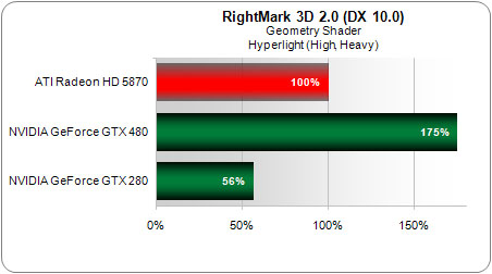
This is an area where the new GeForce GTX 480 has evolved the most compared to the previous architecture, with no less than a 311% improvement in RightMark's Hyperlight.
Finally, the PolyMorph Engine performs the viewport transform and perspective correction calculations before passing the vertices and all of their attributes to the Raster Engine. The Raster Engine is made up of three main stages. First, the equations for the edges of the triangle are calculated, and the triangles that are not facing the camera are rejected. Then, the rasterizer generates the pixels (and the samples in the case of MSAA) covered by the triangle before passing all the data to a Z-Cull unit, now a familiar entity, which avoids performing pixel shading on hidden pixels through the use of a hierarchical Z-buffer.
Reworked ROP Units
As we saw earlier, Nvidia increased the number of ROPs, but it also made a few changes to them. The units' "graphics" performance hasn’t been changed (one 32-bit integer pixel per clock cycle, one FP16 pixel over two clocks, or an FP32 pixel over four clocks), but Nvidia has greatly optimized atomic operations (that is, memory operations carried out in one single transaction) with no interruption possible. This type of operation is extremely useful in parallel programming, when several threads can attempt to access the same resource. Nvidia claims very big gains--up to 20x in the case of atomic operations to a single address and 7.5x for contiguous memory regions, even if, in practice, these gains are probably more the result of using the L2 cache, rather than any substantial modification of the ROP units.
Nvidia also claims a substantial improvement to its compression algorithms, resulting in better efficiency with 8x anti-aliasing.
Get Tom's Hardware's best news and in-depth reviews, straight to your inbox.
Finally, GF100 has a new 32x Coverage Sampling Anti-Aliasing (CSAA) mode and the possibility of combining CSAA and transparency multi-sampling to improve anti-aliasing of transparent surfaces. An interesting detail: until now, the number of pixels generated by the setup engine and the number of ROP units increased together. Now, GF100 has 48 ROP units and its rasterizer can generate only 32 pixels per cycle. That may seem like an odd choice at first, but in practice the latest games usually aren't played on high-end hardware without MSAA, and they often use floating-point frame buffers, thereby imposing a heavier workload on the ROP units, which take several cycles to process the pixels. So, the increase in the number of ROP units is justified, but in certain very simple rendering passes they’ll be underutilized by the rasterizers.
GPGPU
It’s hard to discuss the GF100 without talking about GPGPU, since Nvidia focused on it so much during its presentations of the new architecture. When the company designed G80, the GPGPU market was in its infancy. Nvidia’s choices proved to be good ones, both from the point of view of hardware (with Shared Memory) and software (Compute Shaders and OpenCL have programming paradigms that are very close to CUDA). But it’s impossible to offer a perfect solution on the first try, and Nvidia continues to develop CUDA, adding support for double-precision and atomic instructions with GT200. But those were just incremental improvements. With its Fermi architecture, Nvidia was able to take advantage of all the expertise gained from several years of work with CUDA to offer a much more powerful solution.
The first point that has been greatly improved with GF100, and that will directly benefit GPGPU applications, is support for double-precision arithmetic. As we saw earlier, the addition of double-precision support to the GT200 really looked like a quick and dirty solution, added just to stake out the territory. With a single 64-bit unit compared to eight 32-bit units, the GT200’s double-precision performance wasn’t really up to snuff. Without using dedicated units, AMD was even able to gain the advantage by lowering the performance of its GPU by "only" a factor of four with DP, which was only half the performance hit on Nvidia's architecture.
But with GF100, Nvidia completely reworked the architecture, and the dedicated MAD unit has been done away with. Now, the same units handle single- and double-precision calculation, and performance is reduced only by half with double-precision. So, the impact on performance is much more reasonable comparable to what’s observed on CPUs when using SSE. The advantage of using a GPU for this type of calculation should now be attractive enough to motivate programmers to do the necessary recoding.
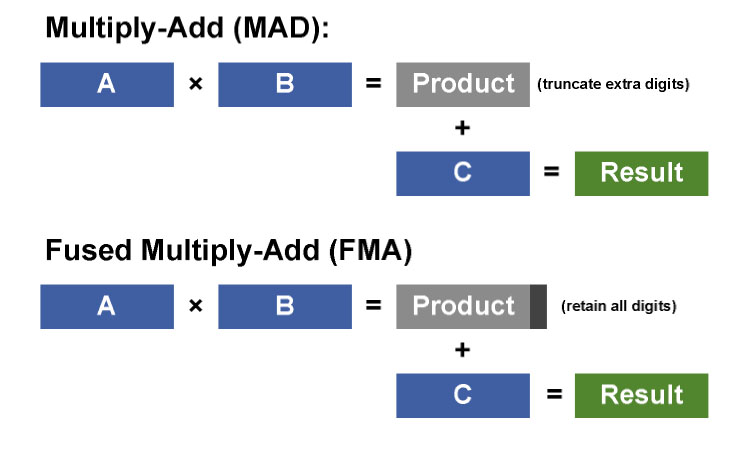
While we’re on the subject of floating-point calculation, note that GF100 supports the most recent IEEE 754-2008 standard, with all of the required rounding algorithms and floating-point multiply-add double (FMAD) instructions. It maintains the precision of the calculation throughout and does only a single rounding, unlike the classic multiplication-addition (MAD) instruction, which performs two roundings. Note, however, that its direct competitor, AMD's RV870, is not really behind in this area because it also supports the latest floating-point standard and the FMAD instruction.
We described another advantage favoring Fermi in GPGPU environments on the previous page: a new memory hierarchy. In certain cases, a little scratchpad RAM can work miracles, but there are situations where nothing can replace cache memory. Also, GF100 has optional support for ECC memory, and all of the GPU’s internal memory (L1 and L2 cache, plus shared memory) is also protected.
Nvidia corrected two bottlenecks that could slow the performance of its chips in GPGPU mode. Like a CPU, a GPU gives the illusion of executing several tasks in parallel by alternating between them, with each task being given a portion of the GPU time. The main difference between CPUs and GPUs is that, on the latter, switching tasks is extremely expensive. Nvidia grappled with this issue in designing GF100, optimizing these operations. Context-switch time is now down to less than 25 microseconds. With that degree of improvement, frequent inter-kernel communication is now feasible where it wasn’t before.
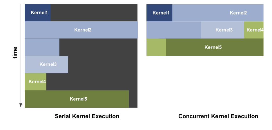
Another big improvement: up until now, the GPU could only execute one kernel at a time on the entire GPU. With large kernels, that wasn’t a problem, and all resources were used. But with small kernels, it was possible for part of the GPU to go unused. GF100 is now capable of executing several kernels in parallel (in practice, up to one per multiprocessor), which results in more efficient use of the GPU, even with large kernels. That’s because when larger kernels reach the end of their execution, it’s possible for them to have an insufficient number of blocks to occupy the entire GPU.
Management of branching has been optimized too, with support for predication instructions. These execute two divergent portions of code in parallel before determining which one is to be kept. This avoids the additional cost of the branching instruction, which can be advantageous when the code to be executed is limited.
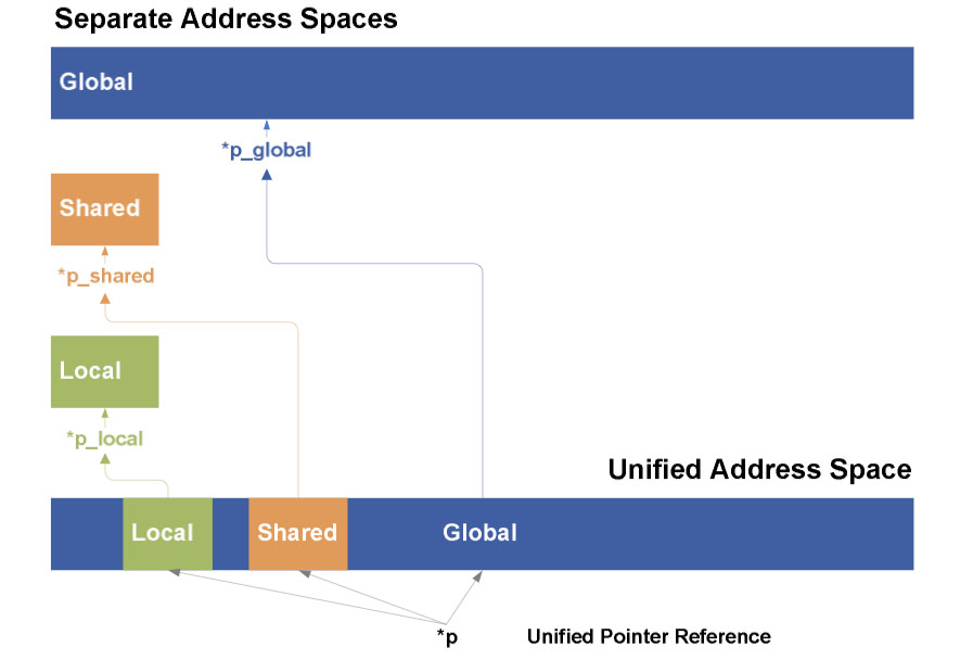
The final new feature is a unified memory space. Until now, PTX ISA 1.0 (the virtual instruction set to which CUDA programs are compiled) had three address spaces: the global, device- and system-wide space, the private local space for each thread, and the space shared by all the threads in a given block. The target of a load/store instruction had to be determined at compile time, which made it difficult to completely implement pointers whose target can change dynamically at run time. With the PTX ISA 2.0 supported by GF100, a single address space is used, which, among other things, makes support for C++ programs possible. C++ objects largely depend on the use of pointers to implement virtual functions, whose behavior can change at run time depending on the dynamic type of the object.
Let’s give credit where credit is due. After several months of stagnation, the little world of 3D has finally awakened, and we now have two Direct3D 11 architectures, designed with quite different approaches.
Current page: Additional Reading: Geometry, Raster, ROP, And GPGPU
Prev Page Additional Reading: Memory Hierarchy, Setup Engine, Tessellation-
restatement3dofted I have been waiting for this review since freaking January. Tom's Hardware, I love you.Reply
With official reviews available, the GTX 480 certainly doesn't seem like the rampaging ATI-killer they boasted it would be, especially six months after ATI started rolling out 5xxx cards. Now I suppose I'll just cross my fingers that this causes prices for the 5xxx cards to shift a bit (a guy can dream, can't he?), and wait to see what ATI rolls out next. Unless something drastic happens, I don't see myself choosing a GF100 card over an ATI alternative, at least not for this generation of GPUs. -
tipoo Completely unimpressed. 6 months late. Too expensive. Power hog. Performance not particularly impressive. The Radeon 5k series has been delivering a near identical experience for 6 months now, at a lower price.Reply
-
tpi2007 hmmm.. so this is a paper launch... six months after and they do a paper launch on a friday evening, after the stock exchange has closed.. smart move by Nvidia, that way people will cool off during the weekend, but I think their stocks won't perform that brilliantly on monday...Reply -
Godhatesusall high power consumption, high prices along with a (small, all things considered) performance edge over ATI is all there is. Are 100$ more for a gtx 480 really worth 5-10% increase in performance?Reply
Though the big downside of fermi are temps. 97 is a very large(and totally unacceptable) temperature level. IMO fermi cards will start dying from thermal death some months from now.
I just wanted competition,so that prices would be lower and we(the consumers) could get more bang for our buck. Surely fermi doesnt help alot in that direction(a modest 30$ cut for 5870 and 5850 from ATI and fermi wont stand a chance). It seems AMD/ATI clearly won this round -
Pei-chen Wow, it seems Nvidia actually went ahead and designed a DX11 card and found out how difficult it is to design. ATI/AMD just slapped a DX11 sticker on their DX10 card and sells it as DX11. In half a year HD 5000 will be so outdated that all it can play is DX10 games.Reply -
outlw6669 Kinda impressed :/Reply
The minimum frame rates are quite nice at least...
Lets talk again when a version with the full 512 SP is released.


