GeForce GTX 480 And 470: From Fermi And GF100 To Actual Cards!
Additional Reading: Breaking Down GF100
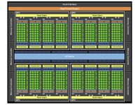
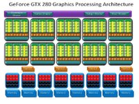
A quick look at the diagram of the GF100 is enough to see extent of the changes in comparison to the GT200.


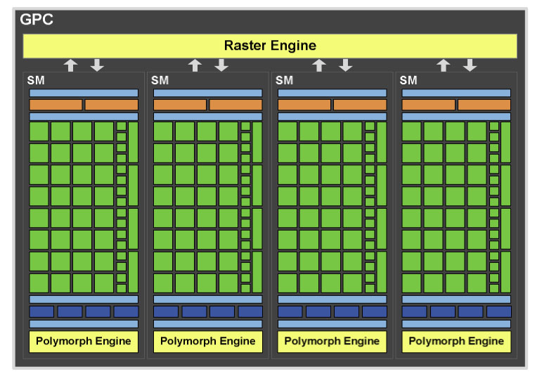
The diagram of the GT200 shows a set of functions shared by the entire GPU, such as the setup engine and the Streaming Processors Array. Conversely, on the GF100, four large Graphics Processing Clusters (GPCs) can be seen, and each GPC is largely independent.
Another remarkable point is the presence of a large L2 cache memory shared by the entire GPU. Now let’s look at the characteristics of the two new cards offered by Nvidia:
| Header Cell - Column 0 | GeForce GTX 480 | GeForce GTX 470 |
|---|---|---|
| Core Clock | 700 MHz | 607 MHz |
| Shader Clock | 1,401 MHz | 1,215 MHz |
| Memory Clock | 924 MHz | 837 MHz |
| CUDA Cores | 480 | 448 |
| Texture Units | 60 | 56 |
| ROPs | 48 | 40 |
Taking into account the final clock frequency of the cores, the processing power works out to 1.344 TFLOPS with FMA (Fused Multiply-Add), compared to 2.72 TFLOPS for AMD's Cypress processor. However, you have to keep in mind that processing power is not everything when it comes to GPUs; it’s only one factor among many. GT200 was technically weaker than RV770 when it came to processing power, but it still dominated it in most games. That’s explained by the fact that the AMD's architecture is less flexible than Nvidia’s in the way it handles instructions in parallel. It uses VLIW units, which require a powerful compiler to extract the parallelism. The trade-off is that AMD can offer a high number of stream processors.
There’s another disappointment: the shader frequency. It has actually been decreased compared to GeForce GTX 285, down to 1,401 MHz from 1,476 MHz. On the other hand, GPU frequency increases from 648 MHz to 700 MHz.
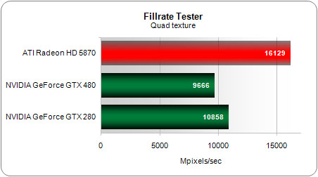
We’ve been critical of AMD on several occasions for its modest texture unit and ROP enhancements, but we’ve never complained about Nvidia. With GF100, for the first time, a new Nvidia GPU actually has fewer texture units than its predecessor (60 compared to 80). But in practice, the units have been reworked, in particular, at the level of the memory subsystem. They're also clocked faster. Still, in certain specific tests, the difference is likely to have a noticeable impact. Let’s look at a simple quad texturing test, for example:
Here we see a difference of -11% between GeForce GTX 480 and GeForce GTX 280, which confirms our theory. On this very simple test, the Radeon HD 5870 is also 67% more powerful than the new Nvidia card. But we’ll get back to that point later.
Get Tom's Hardware's best news and in-depth reviews, straight to your inbox.
Fortunately, there are no unpleasant surprises when it comes to the ROPs. Even though the use of a 384-bit bus (as opposed to a 512-bit interface on GT200) might suggest a reduction in the number of units, Nvidia more than compensates by doubling the number of ROPs per partition. The GT200 had eight partitions with four ROPs each, whereas GF100 now has six partitions of eight, for a total of 48 ROPs, enabling Nvidia to take the advantage back from AMD.
Current page: Additional Reading: Breaking Down GF100
Prev Page Conclusion Next Page Additional Reading: SMs, Scheduler, And Texturing-
restatement3dofted I have been waiting for this review since freaking January. Tom's Hardware, I love you.Reply
With official reviews available, the GTX 480 certainly doesn't seem like the rampaging ATI-killer they boasted it would be, especially six months after ATI started rolling out 5xxx cards. Now I suppose I'll just cross my fingers that this causes prices for the 5xxx cards to shift a bit (a guy can dream, can't he?), and wait to see what ATI rolls out next. Unless something drastic happens, I don't see myself choosing a GF100 card over an ATI alternative, at least not for this generation of GPUs. -
tipoo Completely unimpressed. 6 months late. Too expensive. Power hog. Performance not particularly impressive. The Radeon 5k series has been delivering a near identical experience for 6 months now, at a lower price.Reply
-
tpi2007 hmmm.. so this is a paper launch... six months after and they do a paper launch on a friday evening, after the stock exchange has closed.. smart move by Nvidia, that way people will cool off during the weekend, but I think their stocks won't perform that brilliantly on monday...Reply -
Godhatesusall high power consumption, high prices along with a (small, all things considered) performance edge over ATI is all there is. Are 100$ more for a gtx 480 really worth 5-10% increase in performance?Reply
Though the big downside of fermi are temps. 97 is a very large(and totally unacceptable) temperature level. IMO fermi cards will start dying from thermal death some months from now.
I just wanted competition,so that prices would be lower and we(the consumers) could get more bang for our buck. Surely fermi doesnt help alot in that direction(a modest 30$ cut for 5870 and 5850 from ATI and fermi wont stand a chance). It seems AMD/ATI clearly won this round -
Pei-chen Wow, it seems Nvidia actually went ahead and designed a DX11 card and found out how difficult it is to design. ATI/AMD just slapped a DX11 sticker on their DX10 card and sells it as DX11. In half a year HD 5000 will be so outdated that all it can play is DX10 games.Reply -
outlw6669 Kinda impressed :/Reply
The minimum frame rates are quite nice at least...
Lets talk again when a version with the full 512 SP is released.


