R600: Finally DX10 Hardware from ATI
Get Tom's Hardware's best news and in-depth reviews, straight to your inbox.
You are now subscribed
Your newsletter sign-up was successful
Food For Thought: Reasons For This Design
Looking at ATI's past accomplishments gives a good idea of why it chose to design R600 the way it is. The R500 series introduced dynamic branching in shaders and stream computing in conjunction with the work of Mike Huston at Stanford University (2003-2004) and Folding@Home. With the X1000 series, ATI created new massive and complicated fully associative caches. It added Fetch4, a 2x2 neighborhood fetch performance improvement technique for point-sampling a 16-bit texture in order to perform Precision Closer Filtering (PCF). Lastly, it created a new ring memory controller with a distributed system to allow for 60-70 clients.
Moving from PC to console, ATI worked on the Xenos product for the Xbox 360. While it was not DX10, it was a unified DX9 shader for vertex and pixel shading. The chip had high utilization and added stream out to do after vertex processing. It also incorporated hardware tessellation to take low poly meshes, add more polygons and end up with high poly meshes with higher throughput than strictly using only high poly objects and models.
The New Design - High Level View
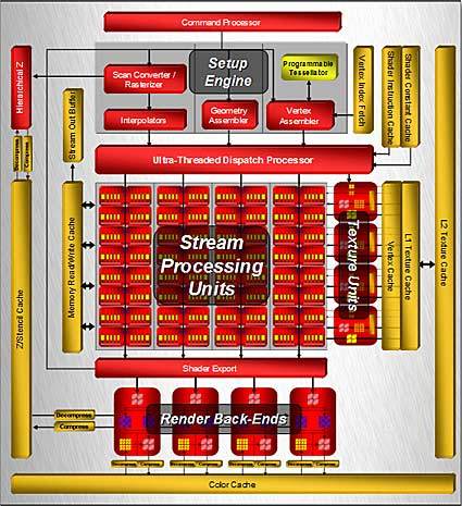
R600 architecture for Radeon HD 2900 (Click for a larger image)
We will start by looking at the core from a bird's eye view and then hone in to focus on each part. Just from looking at the new architecture you should be able to see where ATI leveraged ideas from the previous products. The new dispatch controllers were designed from experiences of the past with pixel scheduling from the 500 series and vertex plus pixel scheduling from Xenos. Full DX10 requires even more scheduling as the geometry shader was added to the mix. In order to handle all of the tasks, virtualizations needed to be added.
There was an old rumor that ATI's upcoming graphics processors would continue to comprise a vector plus scalar instruction design. That is not the case. ATI changed its processor architecture to a super scalar design meaning that scalar instructions are grouped together for blocks of five. AMD Senior Architect Eric Demers stated: "We went to a superscalar design instead of a vector plus scalar because superscalar is more efficient as you can better utilize all of the FPU computes."
ATI uses groups of scalars to form very large instruction words. Is this more efficient than a purely scalar design? It depends. A true scalar approach is simplistic but is shallow. Superscalar can be as deep as its granularity but could get chocked if the instructions are not fed in correctly. This is beyond the scope of this article and we will address the arguments for both designs at another time.
ATI continues to utilize an ultra-threaded dispatch processor to keep all of the chip units busy all of the time. The logic is to have all of the threads working in parallel and to have many different kinds of shaders executing simultaneously. Stalls in the process will only result in poor performance so ATI upped the ante by virtualizing the threads. At any given moment there are only a few hundred in flight, as virtualization effectively allows for an unlimited number of threads. These threads are then fed into four single-instruction multiple-data (SIMD) array paths. All four arrays have one set of instructions going to each one of them and are independent of one another. In all, there are 64 blocks of five streaming processors for a total of 320.
Get Tom's Hardware's best news and in-depth reviews, straight to your inbox.
The architecture has unified shaders. As we have pointed out in our DX10 article last fall and G80 launch article , we demonstrated how a unified shader code in DX10 with unified architecture can increase utilization as well as performance. In games such as Oblivion and many soon to come out, there are very different loads during the frame time. Early on in the frame we are going to see deferred lighting, shadow passes, character animations and a lot of pure vertex processing with relatively small amounts of pixel possessing. Later in the frame, it is typical for a HDR pass, tone mapping, blur filters, tuning, bloom effects, post processing and many other things that are clearly pixel processing.
Located to the right of the shaders/SPs on the diagram, there are four groups of texture units. Each is capable of fetching data with large caches for vertex and texture data as well as a new L2 data cache. Below the shaders are four regular back ends, which ATI claims double the Z-buffering performance from the previous (x1000) generation.
Bandwidth was drastically improved, which is 512-bits wide in both directions. It was not just a task of adding a lot of pins around the outside of the chip. All of the hardware to distribute all of the bandwidth to everything in the chip had to be put in as well. "There are a lot of wires and a lot of transistors," Demers said. "It was a big design decision." Rightly so, as ATI has effectively doubled the bandwidth.
Current page: Food For Thought: Reasons For This Design
Prev Page Was It Worth The Wait? Next Page Meet The Entire Family
