AMD Radeon RX Vega 56 8GB Review
Why you can trust Tom's Hardware
Board Layout & Components
Board Layout
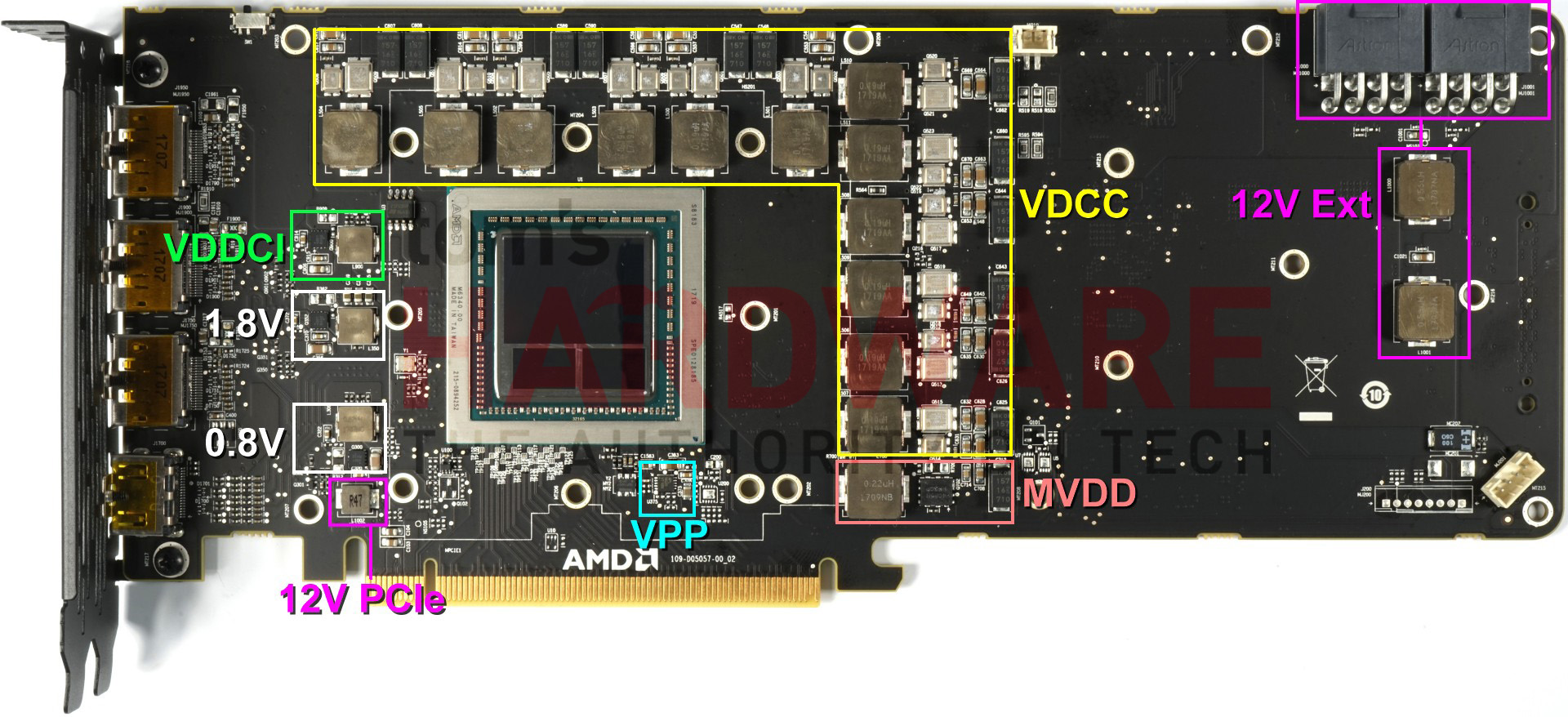
AMD’s RX Vega 64, RX Vega 56, and Vega Frontier Edition employ the exact same board and components. The only differences are the package soldered to the board (this includes HBM2) and adjusted firmware. If AMD wanted to shorten Vega to the length of Radeon R9 Nano, it could.
The lack of memory modules outside of the package opened up some possibilities for AMD to get creative with its PCB. Now, the voltage regulators are found where you'd expect to find GDDR5, and we're looking at a classic 6+1-phase design for power delivery to the GPU and HBM2.
A pair of eight-pin auxiliary power connectors have one coil each; they help smooth out certain voltage peaks. Interestingly, though, there are no large capacitors to be seen.
GPU Power Supply
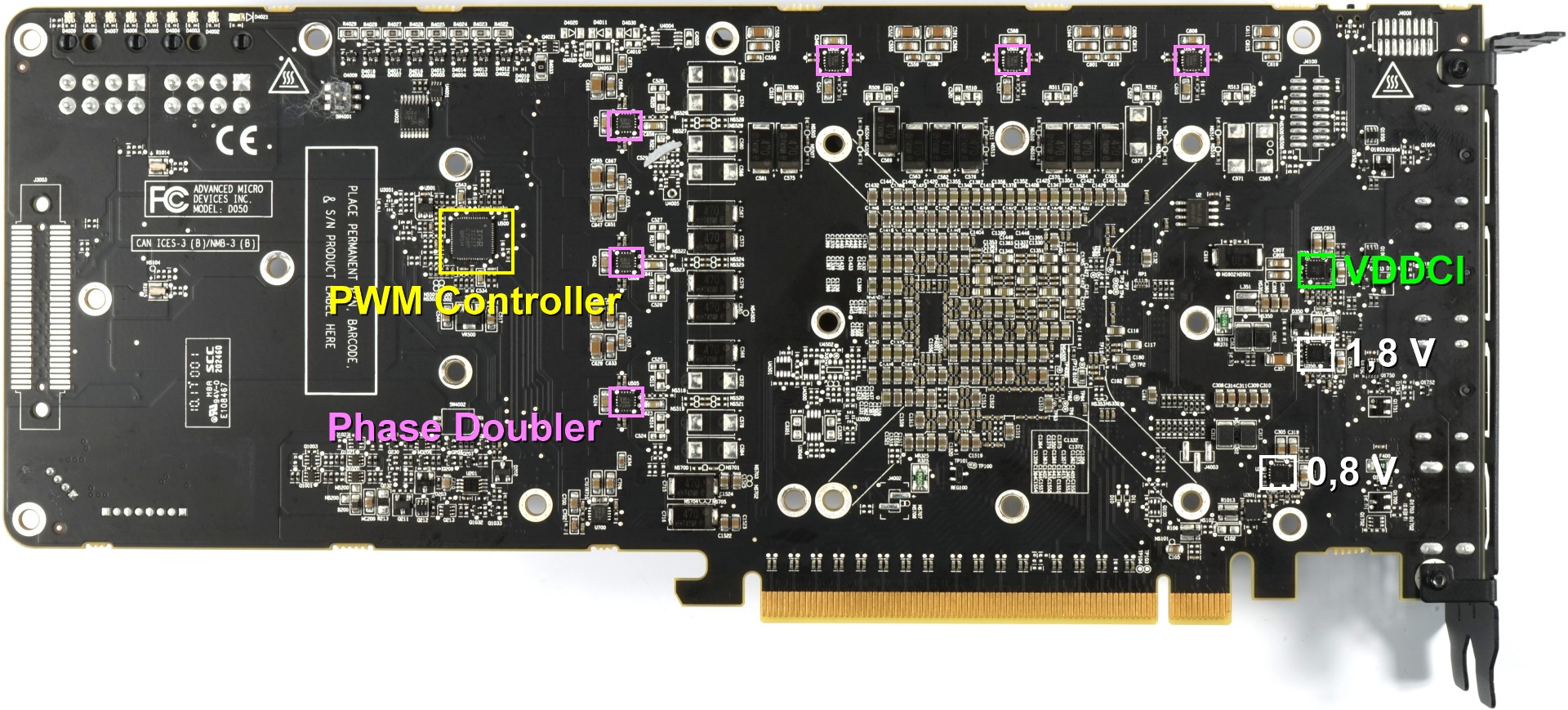
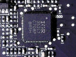
At the center of it all is International Rectifier's IR35217, a poorly-documented dual-output multi-phase controller able to provide six phases for the GPU and two others. A closer look reveals 12 regulator circuits though, not just six. This is a result of doubling, allowing the load from each phase to be distributed between two regulator circuits.
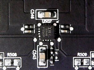
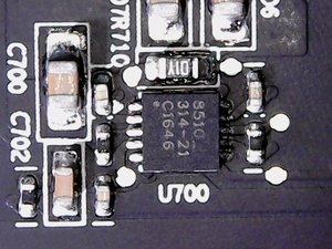
Six IR3598 interleaved MOSFET drivers on the back of the board are responsible for the doubling. These are the parts we pointed out earlier. The following video was taken at idle and shows how the PWM controller switches the load back and forth between the circuits. This keeps efficiency high by using only one phase, but also avoids overloading a single circuit over prolonged periods of time.
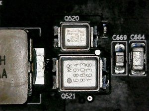
The actual voltage conversion for each of the 12 regulator circuits is handled by an IRF6811 on the high side and an IRF6894 on the low side, which also contains the necessary Schottky diode. Both are International Rectifier HEXFETs that we've seen AMD use before.
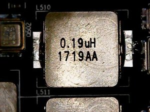
For the coils, AMD went with encapsulated ferrite core chokes that are soldered in the front. At 190nH, their inductivity is a bit lower than the 220nH we often see.
Get Tom's Hardware's best news and in-depth reviews, straight to your inbox.
Memory Power Supply
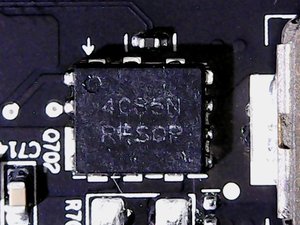
The memory's one phase is supplied by the IR35217 as well. One phase is plenty, since on-package HBM2 needs a lot less power. A CHL815 gate driver is found on the back of the board. For the voltage converters, AMD opted for ON Semiconductor's NTMFD4C85N, a dual N-channel MOSFET that supplies the high and low sides.
It’s interesting that AMD went with flat SMD capacitors instead of can caps. The somewhat lower capacity is compensated for by simply running two of them in parallel on the back of the board. It does make sense to spread the hot-spots and make the thermal solution's job a little easier. Waste heat is kept to a minimum, as is the cost associated with cooling.
At 220nH, the coils are a bit larger this time around. The ones corresponding to the "partial voltage" converters, which operate at a much lower frequency, are even larger at 820nH. They don’t have to deal with the same amounts of power, though.
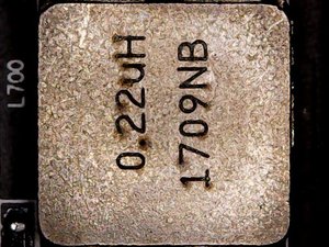
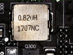
Other Voltage Converters
Creating the VDDCI isn’t a very difficult task. But it's an important one since this regulates the transition between the internal GPU and memory signal levels. It’s essentially the I/O bus voltage between the GPU and the memory. As such, two constant sources of 1.8V and 0.8V are supplied.
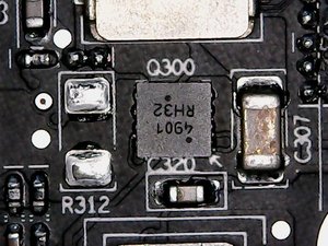
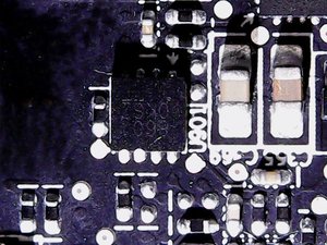
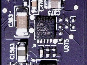
Underneath the GPU, there’s an Anpec APL5620 low drop-out linear regulator, which provides the very low voltage for the phase locked loop (PLL) area.
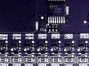
ON Semiconductor's MC74HC238A demultiplexer drives the LED bar that shows the power supply’s load. It’s a fun gimmick, but does get annoying in a dark room at night due to its brightness.
The remaining components are the usual fare.
MORE: Best Graphics Cards
MORE: Desktop GPU Performance Hierarchy Table
MORE: All Graphics Content
Current page: Board Layout & Components
Prev Page Disassembly, Cooler & Interposer Next Page How We Tested AMD's Vega RX 56 8GB-
kjurden What a crock! I didn't realize that Tom's hardware pandered to the iNvidiot's. AMD VEGA GPU's have rightfully taken the performance crown!Reply -
Martell1977 Vega 56 vs GTX 1070, Vega goes 6-2-2 = Winner Vega!Reply
Good job AMD, hopefully next gen you can make more headway in power efficiency. But this is a good card, even beats the factory OC 1070. -
Wisecracker Thanks for the hard work and in-depth review -- any word on Vega Nano?Reply
Some 'Other Guys' (Namer Gexus?) were experimenting on under-volting and clock-boosting with interesting results. It's not like you guys don't have enough to do, already, but an Under-Volt-Off Smack Down between AMD and nVidia might be fun for readers ...
-
pavel.mateja No undervolting tests?Reply
https://translate.google.de/translate?sl=de&tl=en&js=y&prev=_t&hl=de&ie=UTF-8&u=https://www.hardwareluxx.de/index.php/artikel/hardware/grafikkarten/44084-amd-radeon-rx-vega-56-und-vega-64-im-undervolting-test.html&edit-text= -
10tacle Reply20112576 said:What a crock! I didn't realize that Tom's hardware pandered to the iNvidiot's. AMD VEGA GPU's have rightfully taken the performance crown!
Yeah Tom's Hardware does objective reviewing. If there are faults with something, they will call them out like the inferior VR performance over the 1070. This is not the National Inquirer of tech review sites like WCCTF. There are more things to consider than raw FPS performance and that's what we expect to see in an honest objective review.
Guru3D's conclusion with caveats:
"For PC gaming I can certainly recommend Radeon RX Vega 56. It is a proper and good performance level that it offers, priced right. It's a bit above average wattage compared to the competitions product in the same performance bracket. However much more decent compared to Vega 64."
Tom's conclusion with caveats:
"Even when we compare it to EVGA’s overclocked GeForce GTX 1070 SC Gaming 8GB (there are no Founders Edition cards left to buy), Vega 56 consistently matches or beats it. But until we see some of those forward-looking features exposed for gamers to enjoy, Vega 56’s success will largely depend on its price relative to GeForce GTX 1070."
^^And that's the truth. If prices of the AIB cards coming are closer to the GTX 1080, then it can't be considered a better value. This is not AMD's fault of course, but that's just the reality of the situation. You can't sugar coat it, you can't hide it, and you can't spin it. Real money is real money. We've already seen this with the RX 64 prices getting close to GTX 1080 Ti territory.
With that said, I am glad to see Nvidia get direct competition from AMD again in the high end segment since Fury even though it's a year and four months late to the party. In this case, the reference RX 56 even bests an AIB Strix GTX 1070 variant in most non-VR games. That's promising for what's going to come with their AIB variants. The question now is what's looming on the horizon in an Nvidia response with Volta. We'll find out in the coming months. -
shrapnel_indie We've seen what they can do in a factory blower configuration. Are board manufacturers allowed to take 64 and 56 and do their own designs and cooling solutions, where they can potentially coax more out of it (power usage aside)? Or are they stuck with this configuration as Fury X and Fury Nano were stuck?Reply -
10tacle No, there will be card vendors like ASUS, Gigabyte, and MSI who will have their own cooling. Here's a review of an ASUS RX 64 Strix Gaming:Reply
http://hexus.net/tech/reviews/graphics/109078-asus-radeon-rx-vega-64-strix-gaming/ -
pepar0 Reply
Will any gamers buy this card ... will any gamers GET to buy this card? Hot, hungry, noisy and expensive due to the crypto currency mining craze was not what this happy R290 owner had in mind.20112412 said:Radeon RX Vega 56 should be hitting store shelves with 3584 Stream processors and 8GB of HBM2. Should you scramble to snag yours or shop for something else?
AMD Radeon RX Vega 56 8GB Review : Read more
