Xotic PC NP9150: Striking Back At Kepler With Radeon HD 7970M
We've seen the efficiency of Nvidia's Kepler architecture first-hand on the desktop. But AMD's Radeon HD 7970M pulls off a stellar showing in Xotic PC's Sager NP9150 notebook, reminding everyone that even a Pitcairn-based flagship packs a serious punch.
AMD's Radeon HD 7970M, Exposed
We already examined Clevo’s P150EM in Eurocom Racer 2.0 Review: Intel's Ivy Bridge Meets Nvidia's Kepler, though Sager, a distributor of Clevo's whitebook designs, renames it to the NP9150 before it gets to Xotic PC. Aside from the logos, it’s the same chassis.
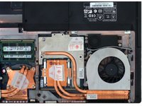
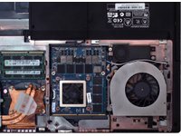
Opening up the machine reveals very similar cooling to what we saw on Nvidia's GeForce GTX 660M. The Radeon HD 7970M has the same basic cooler design as the GeForce, but with custom-matched contact surfaces.


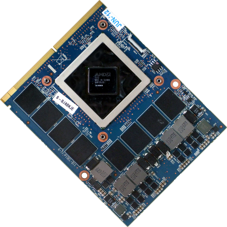
The Radeon HD 7970 GPU is composed of nearly three billion transistors, and it takes up much of the graphics module's real estate, even in light of TSMC's 28 nm manufacturing process. But isn't AMD's Radeon HD 7970 supposed to have 4.3 billion transistors?
Article continues below| Desktop vs Mobile Radeon Graphics | |||
|---|---|---|---|
| Row 0 - Cell 0 | Desktop Radeon HD 7970 | Radeon HD 7970M | Desktop Radeon HD 7870 |
| Architecture | Tahiti | Pitcairn | Pitcairn |
| Transistors | 4.3 billion | 2.8 billion | 2.8 billion |
| Engine Clock | 925 MHz | 850 MHz | 1000 MHz |
| Stream Processors | 2048 | 1280 | 1280 |
| Texture Units | 128 | 80 | 80 |
| ROP Units | 32 | 32 | 32 |
| Compute Performance | 3.79 TFLOPS | 2.18 TFLOPS | 2.56 TFLOPS |
| DRAM Type | GDDR5-5500 | GDDR5-4800 | GDDR5-4800 |
| DRAM Interface | 384-bit | 256-bit | 256-bit |
| Memory Bandwidth | 264 GB/s | 154 GB/s | 154 GB/s |
| TDP | 250 W | 75 W | 175 W |
The Radeon HD HD 7970M obviously doesn't boast the Tahiti core with which its model name is most commonly associated. Rather, it's a more power-optimized version of the same Pitcairn GPU found in the desktop Radeon HD 7870. It’s not all bad that AMD chose a smaller die for its flagship mobile GPU, we just wish it had picked a more appropriate name. At least they’re both current-generation parts based on a 28 nm node.
| Desktop vs Mobile GeForce Graphics | |||
|---|---|---|---|
| Row 0 - Cell 0 | Desktop GeForce GTX 670 | GeForce GTX 675M | Desktop GeForce GTX 560 Ti |
| Architecture | Kepler (GK104) | Fermi (GF114) | Fermi (GF114) |
| Transistors | 3.54 billion | 1.95 billion | 1.95 billion |
| Engine Clock | 915 MHz | 620 MHz | 822 MHz |
| Cuda Cores | 1344 | 384 | 384 |
| Texture Units | 112 | 64 | 64 |
| ROP Units | 32 | 32 | 32 |
| Compute Performance | 2.46 TFLOPS | 952 GFLOPS | 1.26 TFLOPS |
| DRAM Type | GDDR5-6008 | GDDR5-3000 | GDDR5-4008 |
| DRAM Interface | 256-bit | 256-bit | 256-bit |
| Memory Bandwidth | 192 GB/s | 96 GB/s | 128 GB/s |
| TDP | 170 W | 100 W | 170 W |
By comparison, Nvidia’s GeForce GTX 675M isn’t even part of the same generation. Its GeForce GTX 560 Ti (based on the Fermi architecture at 40 nm) was a top value in its day, but even that card was replaced long ago by a more-powerful 448-core version. We’d like to come down harder on AMD for its naming tomfoolery, but Nvidia is the guiltier party in this specific case.
Get Tom's Hardware's best news and in-depth reviews, straight to your inbox.
Current page: AMD's Radeon HD 7970M, Exposed
Prev Page Can Xotic PC Provide More Value? Next Page System And Benchmark Configurations-
Did the test show any sign of 7970M utilization issue? It is a well known problem reported by many members from Notebookreview forum.Reply
-
Crashman QKVenGenDid the test show any sign of 7970M utilization issue? It is a well known problem reported by many members from Notebookreview forum.Care to elaborate?Reply -
sherlockwing CrashmanCare to elaborate?Reply
If I recall it is a Enduro related bug causing 7970M to be under utilized in games like BF3, it was quite a big deal in June/July on NotebookReview's Forum, not sure if it is fixed by new drivers. -
EzioAs I find it hard to believe that the 7970M performs a bit too well in Battlefield 3. Even the 7870 and 660ti gets lower fps with the same settings at 1080p.Reply
http://www.tomshardware.com/reviews/geforce-gtx-660-geforce-gtx-650-benchmark,3297-7.html -
No games on 7970m doesant play fine. Most of them are affected by enduro underutilizaiotn which basicly causes the card to notutilize fully when lowering settings in games. For example , in bf 3 multiplayer( as there is no problem in singleplayer) when you enter a lrger map with 64p on it, youl get around 35 fps maxed but with dips down to 25 fps which is not enought for a fast paced shotter. So when setting are lowered you expect to get better fps right?? thats not the case with 7970m- the fps remains the same but utilization of the card drops down. This also happens in many other games that are sometimes even unplayable. You just cant achieve stable 60 fps no matter what settings- the lower the settings go, the lower the card utilization is. There is a logging thread, and many other threads regarding this issue on notebookreview. Amd adressed that there is a driver coming soon, but for users that have this card form half a year now its taking pretty long..Reply
-
I concur what Mahalsk said. A 7970M in a EM-series Clevo laptop IS NOT A GOOD DEAL for the price they are asking, since the card doesn't work properly. This is the case with all EM-series laptops and all 7970Ms out there. Even the 6900M series of AMD cards are beating 7970M at the moment with the Enduro issue unsolved.Reply
Check this thread (and the "Sager and Clevo forums") for more details:
http://forum.notebookreview.com/sager-clevo/682097-7970m-logging-thread-games-utilization-issues-only-post-logs-no-questions-please.html
, and AVOID 7970M for now. Its been months and no fix from either AMD or Clevo. You do not get what you pay for when bying this configuration. -
montage CrashmanBF3 results look fine to meReply
You didn't test BF3 multiplayer wwith 64 players? The single player works fine, but the multiplayer suffers from enduro issues. Here are some screenshots taken by me:
http://imageshack.us/photo/my-images/716/bf320120727225130242.jpg/
18 fps is not fine in my opinion. Also got 8 fps at times in Civ 5. I have a P170EM Clevo with 3610Qm and 7970M. Anandtech also posted an article concerning Enduro, and they weren't aware of Enduro issues either, but when the people from Notebook review informed them about it, they were able to reproduce the issues. They also edited their article to include a mention about the issue.
The issue is real, and affect all AMD 7000M seriers card that are in laptops which have no MUX-cable. This cable allows a user to use only the dedicated GPU instead of the iGPU. When there is no MUX, the image is always forced through the iGPU, and the Enduro technology that is supposed to make this happen is broken. With Alienware's laptops that have MUX, you can force Enduro off and the issue goes away. If you enable Enduro in AW, the issue comes back.
What you get is sudden FPS drops, stuttering, low GPU utilization. It does not affect every game, but I'd still say its present in most games, e.g. witcher 1 & 2, crysis 2, BF3 multiplayer (more evident on certain maps), GTA 4, etc. etc. (the list goes on).
When you try to reduce the graphics level to get better fps, you only get lower GPU utilization and the same fps. Now this is a serious issue to people playing online shooting games and other competitive games.
Notebook review forums have numerous threads about the issue, and we have been following how the situation develops for months now. So far, AMD has been very silent regarding fixes to these Enduro related issues. -
Link to the Anandtech article:Reply
http://www.anandtech.com/show/6243/amds-enduro-switchable-graphics-levels-up/5
Check the comments and the last 'update' part of the article. This card has been out for almost half a year now with broken switching software.


