432-Core Chiplet-Based RISC-V Chip Nearly Ready to Blast Into Space
ESA taps RISC-V for AI and HPC chip.

The Occamy processor, which uses a chiplet architecture, packs 432 RISC-V and AI accelerators and comes with 32GB of HBM2E memory, has taped out. The chip is backed by the European Space Agency and developed by engineers from ETH Zürich and the University of Bologna, reports HPC Wire.
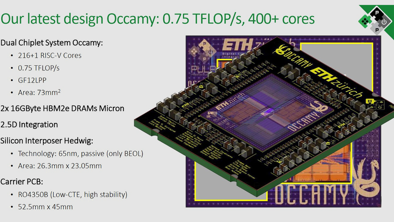
The ESA-backed Occamy processor uses two chiplets with 216 32-bit RISC-V cores, an unknown number of 64-bit FPUs for matrix calculations, and carries two 16GB HBM2E memory packages from Micron. The cores are interconnected using a silicon interposer, and the dual-tile CPU can deliver 0.75 FP64 TFLOPS of performance and 6 FP8 TFLOPS of compute capability.
Neither ESA nor its development partners have disclosed the Occamy CPUs' power consumption, but it is said that the chip can be passively cooled, meaning it might be a low-power processor.

Each Occamy chiplet has 216 RISC-V cores and matrix FPUs, totaling around a billion transistors spread over 73mm^2 of silicon. The tiles are made by GlobalFoundries using its 14LPP fabrication process.
The 73mm^2 chiplet isn't a particularly large die. For example, Intel's Alder Lake (with six high-performance cores) has a die size of 163 mm^2. As far as performance is concerned, Nvidia's A30 GPU with 24GB of HBM2 memory delivers 5.2 FP64/10.3 FP64 Tensor TFLOPS as well as 330/660 (with sparsity) INT8 TOPS.
Meanwhile, one of the advantages of chiplet designs is that ESA and its partners from ETH Zürich and the University of Bologna can add other chiplets to the package to accelerate certain workloads if needed.
The Occamy CPU is developed as a part of the EuPilot program, and it is one of many chips that the ESA is considering for spaceflight computing. However, there are no guarantees that the process will indeed be used onboard spaceships.
The Occamy design aims to support high-performance and AI workloads through a bare-metal runtime, but it is not yet clear whether the runtime will be at a container level or at the bare-metal level. The Occamy processor can be emulated on FPGAs. The implementation has been tested on two AMD Xilinx Virtex UltraScale+ HBM FPGAs and the Virtex UltraScale+ VCU1525 FPGA.
Get Tom's Hardware's best news and in-depth reviews, straight to your inbox.

Anton Shilov is a contributing writer at Tom’s Hardware. Over the past couple of decades, he has covered everything from CPUs and GPUs to supercomputers and from modern process technologies and latest fab tools to high-tech industry trends.
-
bit_user Replythe dual-tile CPU can deliver 0.75 FP64 TFLOPS
In absolute terms, that's really not impressive, especially if it includes dedicated matrix-multiply hardware.
"The top-bin Epyc 9654 part comes in a 320-400 watt TDP and provides 5.38 teraflops of peak double-precision performance running at max boost frequency of 3.5 GHz"Source: https://www.hpcwire.com/2022/11/10/amds-4th-gen-epyc-genoa-96-5nm-cores-across-12-compute-chiplets/
So, it can only win on FLOPS/W or FLOPS/mm^2. And even on those terms, I don't expect it will hold a candle to HPC GPUs.
The tiles are made by GlobalFoundries using its 14LPP fabrication process.
Hmmm... I guess we should compare it to 1st gen EPYC, then. Data on that is much harder to find, but this paper measured 1.03 TFLOPS on dual 32-core Naples system (in contrast, I think the above figures are theoretical).
What might make all the difference is fault-tolerance. Depending on how they handle that, it could further explain the performance delta.
I'd love to know more about the actual cores they used. -
InvalidError "An unknown number of FPUs"Reply
There aren't too many options: 0.75 TFLOPs / 432 total cores / 1 FLOP/cycle = 1.744GHz.
Looks like the CPU has only one FMA64 unit per core assuming it runs at 1.8-2GHz with near 100% occupancy, two if it runs slower or at a much lower unit utilization rate. -
kjfatl To some, this might not seem impressive, but it is intended for a space bases application where it must be radiation hardened. Cosmic rays do nasty things to standard electronics.Reply -
InvalidError Reply
I doubt that a 432 cores CPU will be used to run any operations-critical equipment. Non-essential stuff where occasional crashes and errors are only a minor inconvenience don't need to be radiation-hardened.kjfatl said:To some, this might not seem impressive, but it is intended for a space bases application where it must be radiation hardened. Cosmic rays do nasty things to standard electronics.
Also, to cram 216 cores in 73sqmm, they are almost certainly using high-density libraries instead of radiation-hardened ones. -
bit_user Reply
FMA is usually counted as 2 ops. Then again, its throughput could be 0.5 per cycle, still resulting in 1 FLOP/cycle.InvalidError said:There aren't too many options: 0.75 TFLOPs / 432 total cores / 1 FLOP/cycle = 1.744GHz.
Looks like the CPU has only one FMA64 unit per core assuming it runs at 1.8-2GHz with near 100% occupancy, two if it runs slower or at a much lower unit utilization rate. -
kjfatl Reply
I agree that is is highly unlikely that this part will be used in a critical system. I'm also making the assumption that some level of radiation hardening is needed to keep from getting latch-up conditions that would damage the silicon. It's probably done is a library that has some level of increased radiation hardening. A few glitches in an image are no big deal. Gates that turn into SCRs are a big deal.InvalidError said:I doubt that a 432 cores CPU will be used to run any operations-critical equipment. Non-essential stuff where occasional crashes and errors are only a minor inconvenience don't need to be radiation-hardened.
Also, to cram 216 cores in 73sqmm, they are almost certainly using high-density libraries instead of radiation-hardened ones.
It will be interesting if the ESA publishes this sort of detail. -
bit_user Speaking of radiation hardening, I thought it was fascinating that NASA's Ingenuity drone used a standard Snapdragon 801 phone SoC.Reply
https://en.wikipedia.org/wiki/Ingenuity_(helicopter)
I think that's because all it had to do was demonstrate controlled flight was possible, and its core mission would be considered successful. Furthermore, getting enough compute power into a radiation-hardened package for autonomous flight might've been a challenge.
Meanwhile, the Perseverance rover was plodding along with a ~20-year-old 133 MHz PowerPC CPU.
https://en.wikipedia.org/wiki/Perseverance_(rover)#Design
BTW, the panoramic photos Perseverance captured are of stunning resolution and clarity. I cropped and scaled one down to use as wallpaper, for my multi-monitor setup. It's not the most picturesque landscape, but it really gives the feeling of what it'd be like to stand on Mars. -
Steve Nord_ In space, noone can hear your screaming overclocked APU serve 130 shards of conference? Which of derβauer's cats is going? It's going to juggle a bunch of neodymium magnets around Mars and let it accumulate an atmosphere again?Reply -
kgf_ethz I am part of the team that has designed Occamy. While we are very happy that our project has gotten some attention, the article (and the HPCWire article that started this) is not accurate and have misrepresented several parts. We wrote a short article explaining the background and what Occamy is and isn't:Reply
https://pulp-platform.org/occamy/ We would love to send our designs into space, and we hope we will also get there at some point, but Occamy is not designed for Space, or in collaboration with ESA, it is not a product, and we do not think it can be passively cooled when running at full speed. -
bit_user Reply
Thanks!kgf_ethz said:I am part of the team that has designed Occamy. While we are very happy that our project has gotten some attention, the article (and the HPCWire article that started this) is not accurate and have misrepresented several parts. We wrote a short article explaining the background and what Occamy is and isn't:
This part jumped out at me:
"Each chiplet has a private 16GB high-bandwidth memory (HBM2e) and can communicate with a neighboring chiplet over a 19.5 GB/s wide, source-synchronous technology-independent die-to-die DDR link."So, I'm guessing you get like 1 TB/s of HBM2e bandwidth, but you're limited to like 1/50th of that for die-to-die communication? So, then are they even cache-coherent? Or, is it the idea basically "cluster on a chip"?
It looks like each group of cores has ScratchPad Memory ("SPM"). How fast do they access it? I'm guessing it's entirely software-managed? Are accesses to it cache-coherent, between the cores in the group? The architecture seems design for very tight-collaboration of cores in a group, so I'm guessing you want a more efficient way for them to communicate than relying on whatever level of the cache hierarchy they have in common.
The pairing of 8 SIMD cores with one communication & coordination core seems reminiscent of IBM's Cell, BTW. Was there any thought given to that, or you basically just ended up at the same place?
Also, what's ZMem?